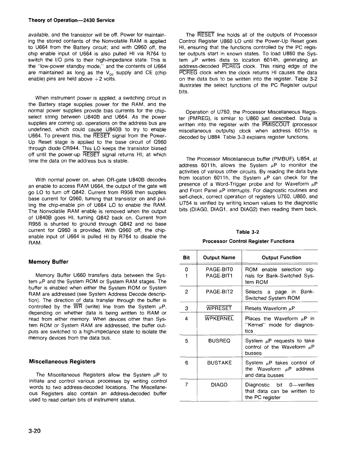
Bit Output Name
Output Function
0
PAGE-BITO ROM enable selection sig-
1 PAGE-BIT1 nals for Bank-Switched Sys-
tem ROM
2 PAGE-BIT2 Selects
a
page in
Bank-
Switched System ROM
3
WPRESET Resets Waveform pP
4 WPKERNEL Places the Waveform J.LPin
"Kernel" mode for diagnos-
tics
5 BUSREO System J.LPrequests to take
control of the Waveform J.LP
busses
6 BUSTAKE System J.LPtakes control of
the
Waveform
J.LP
address
and data busses
7
DIAGO Diagnostic bit O-verifies
that data can be
written to
the PC register
Table 3-2
Processor Control Register Functions
The Processor Miscellaneous buffer (PMBUF), U854, at
address 6011h, allows the System «P to monitor the
activities of various other circuits. By reading the data byte
from location 6011h, the System pP can check for the
presence of a Word-Trigger probe and for Waveform J.LP
and Front Panel J.LPinterrupts. For diagnostic routines and
self-check, correct operation of registers U760, U860, and
U754 is verified by writing known values to the diagnostic
bits (DIAGO, DIAG1, and DIAG2) then reading them back.
Operation of U760, the Processor Miscellaneous Regis-
ter (PMREG), is similar to U860 just described. Data is
written into the register with the PMISCOUT (processor
miscellaneous outputs) clock when address 6015h is
decoded by U884. Table 3-3 explains register functions.
The RESET line holds all of the outputs of Processor
Control Register U860 La until the Power-Up Reset goes
HI, ensuring that the functions controlled by the PC regis-
ter outputs start in known states. To load U860 the Sys-
tem pP writes data to location 6014h, generating an
address-decoded PCREG clock. This rising edge of the
PCREG clock when the clock returns HI causes the data
on the data bus to be written into the register. Table 3-2
illustrates the select functions of the PC Register output
bits.
3-20
The Miscellaneous Registers allow the System pP to
initiate and control various processes by writing control
words to two address-decoded locations. The Miscellane-
ous Registers also contain an address-decoded buffer
used to read certain bits of instrument status.
Miscellaneous Registers
Memory Buffer U660 transfers data between the Sys-
tem pP and the System ROM or System RAM stages. The
buffer is e'nabledwhen either the System ROM or System
RAM are addressed (see System Address Decode descrip-
tion). The direction of data transfer through the buffer is
controlled by the WR (write) line from the System pP,
depending on whether data is being written to RAM or
read from either memory. When devices other than Sys-
tem ROM or System RAM are addressed, the buffer out-
puts are switched to a high-impedance state to isolate the
memory devices from the data bus.
Memory Buffer
With normal power on, when OR-gate U840B decodes
an enable to access RAM U664, the output of the gate will
go La to turn off
0842.
Current from R956 then supplies
base current for
0960,
turning that transistor on and pul-
ling the chip-enable pin of U664 La to enable the RAM.
The Nonvolatile RAM enable is removed when the output
of U840B goes HI, turning
0842
back on. Current from
R956 is shunted to ground through
0842
and no base
current for
0960
is provided. With
0960
off, the chip-
enable input of U664 is pulled HI by R764 to disable the
RAM.
When instrument power is applied, a switching circuit in
the Battery stage supplies power for the RAM, and the
normal power supplies provide bias currents for the chip-
select string between U840B and U664. As the power
supplies are coming up, operations on the address bus are
undefined, which could cause U840B to try to enable
U664. To prevent this, the RESET signal from the Power-
Up Reset stage is applied to the base circuit of
0960
through diode CR944. This La keeps the transistor biased
off until the power-up RESET signal returns HI; at which
time the data on the address bus is stable.
available, and the transistor will be off. Power for maintain-
ing the stored contents of the Nonvolatile RAM is applied
to U664 from the Battery circuit; and with
0960
off, the
chip enable input of U664 is also pulled HI via R764 to
switch the I/O pins to their high-impedance state. This is
the "low-power standby mode," and the contents of U664
are maintained as long as the Vee supply and CE (chip
enable) pins are held above +2 volts.
Theory of Operation-2430 Service