3-21
The Waveform ~P memory space is accessibleby the
System liP, allowingthe System liP to send commandsto
the Waveform ~P and to read any desired result or data
locationespeciallyfor the GPIB
1(0
functions.
The Waveform ProcessorSystem (diagram2) performs
the high-speed data-handling operations needed to pro-
duce and update displays of acquired data points on the
crt including averaging, enveloping, adding, multiplying,
and interpolation of the waveform data. It accepts task
information from the System ~P and then carries out the
assigned tasks without further need of the System liP.
When that task list has been completed,it sendsan inter-
rupt to the System ~P to inform it that another list of
tasks can be accepted.
WAVEFORM PROCESSOR SYSTEM
BATTERY WARNING CIRCUIT. Operational amplifier
U940A is a very high impedance buffer to limit current
drain of the battery. Its bufferedoutput voltage is applied
to the Front Panel~P (diagram3) to monitor for both low-
voltage and over-voltage conditions of the lithium backup
battery. A battery-error condition found at power-on or
with the Extended Diagnostics will cause the BATT-
STATUS test to fail. That test may then be selectedto run
at the next lower levelin the test hierarchyto determineif
the battery is undervoltageor overvoltage. The warning
circuit is operationalonly when normalinstrumentpower is
applied. Resistor RS02 provides additional circuit
impedance that prevents any appreciable discharging of
the battery by the voltage-sensingcircuit.
The eventual charge loss from capacitor C904 causes
its output voltage to drop below that of Backup Battery
ST800 (a lithium battery), and diode CR900 again
becomes reverse biased.The standby current for U664 is
then suppliedfrom the battery via CR802(and R900in the
return path). Diode CR802 acts as the current switch and
prevents reversecurrent through the lithium battery during
normal power-on operation. Resistor R900 provides
reverse-currentlimiting in the event that CRS02becomes
shorted.
With instrument power turned off, transistors 0806 and
Q804 are both turned off. The positive charge potential
stored by capacitor C904 forward biases CR900 and pulls
the chip-enablepin of U664 HI through R764. This dis-
ables RAM U664 and switches its
1(0
ports to high-
impedancestates. Operationin this state is the "standby"
mode in which data in U664 is maintainedusing minimal
supplycurrent.
Theory of Operation-2430 Service
With normal instrument power applied,transistor OS06
will be turned on by the base-bias voltage-dividercircuit
formed by RS12and RS15.Base current is then supplied
through 0806 and R800 to turn on 0804. This is the nor-
mal operating mode,and operating current for Nonvolatile
RAM U664 is supplied via OS04from the+5 Vo supply.
During normal operation, capacitor C904 is held charged
through CR902 but isolated from the RAM power source
by reverse-biaseddiodeCR900.
The Battery circuit suppliesstandby power to the Non-
volatile RAM that allows instrument calibration constants
and front-panel settings to remain stored for long periods
of time (greater than three years) when instrument power
is turned off. A switching circuit turns off the battery
(BT800) current source while normal instrument power is
applied.A battery monitor circuit warns the Front Panel~P
(and thereby the user) of a low-voltage condition (indicat-
ing that it is time to changethe battery)or an over-voltage
condition (indicatingthat reverse current is attempting to
chargethe lithiumbattery).
Battery
If both His and LOs can be written to and read from these
diagnostic locations,fairly high confidencemay be placed
in the addressingand selection of the registers and their
data paths.
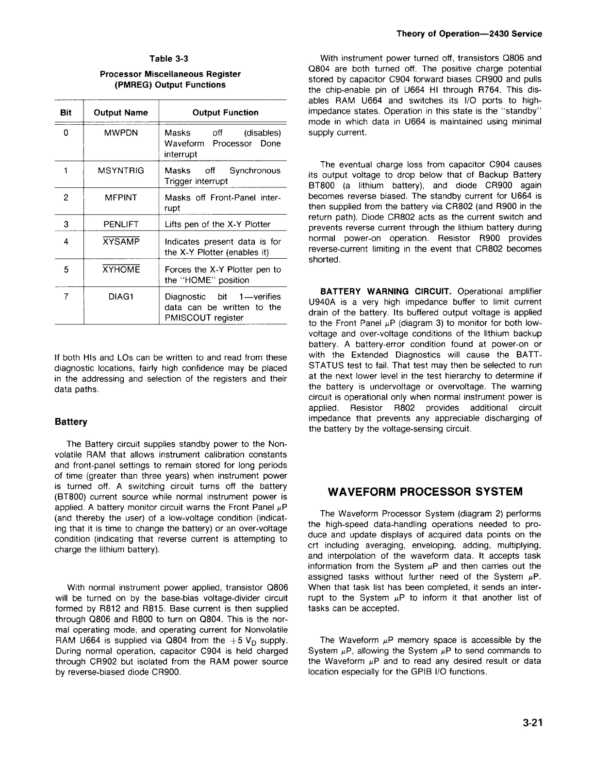
Bit Output Name
Output Function
0
MWPDN Masks off (disables)
Waveform Processor Done
interrupt
1 MSYNTRIG Masks off Synchronous
Trigger interrupt
2 MFPINT Masks off Front-Panel inter-
rupt
3
PENLIFT Lifts pen of the X-Y Plotter
4 XYSAMP
Indicates present data is for
the X-Y Plotter (enablesit)
5 XYHOME
Forcesthe X-Y Plotter pento
the "HOME" position
7 DIAG1 Diagnostic bit 1-verifies
data can be written
to the
PMISCOUTregister
Table 3-3
Processor Miscellaneous Register
(PMREG) Output Functions