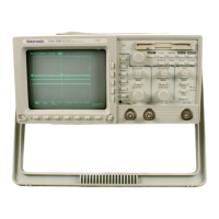
Theory of Operation-314 Service
Input Attenuator
change is accomplished by changing the value of the gain-
The channel 1 deflection factor is determined by the CH
1
VOLTS/DIV switch.
The basic deflection factor of the vertical deflection
system is 10
m/Div in the ten positions of the VOLTS/DIV
switch above 5 m, In the 1, 2, and 5 m positions of the
VOLTS/DIV switch, the basic deflection factor is 1 m/Div.
For VOLTS/DIV switch positions other than 1 m/Div and
10 m/Div, attenuators are switched into the circuit to
produce the vertical deflection factors indicated on the
front panel. These attenuators are frequency-
compensated voltage dividers. In addition to providing
constant attenuation at all frequencies within the
bandwidth of the instrument, the input attenuators are
designed to maintain the same input RC characteristics
(one megohm and approximately 47 picofarads) for each
setting of the
VOLTWDIV switch. Each attenuator con-
tains an adjustable series capacitor to provide correct
attenuation at high frequencies and an adjustable shunt
capacitor to provide correct input capacitance.
5
Division Calibrator
Switching either VOLTS/DIV switch to 5 DIV CAL
provides a five-division (at approximately
1
kilohertz)
display on the crt. The calibrator square-wave amplitude is
accurate enough to permit vertical gain calibration. This
calibrator signal also appears at the .5 V CAL OUT jack
(on the front panel) for compensating attenuator probes
(see Diagrams 1 and
6).
lnput Stage
Channel 1 signal from the input attenuator is connected
to the input stage through C22, R226, and R22A. R23
provides the input resistance
forthis stage. R22A limits the
current drive to the gate of
Q25. CR23 and CR24 protect
the circuit by clamping the gate of
Q25A at about
+6
or
-6
volts if a high-amplitude signal is applied to the CH 1
input connector. Q25B is a relatively constant-current
source and provides temperature compensation for Q25A.
Preamp Stage
The Preamp stage, U40, is a multiple-stage integrated-
circuit amplifier. Adjusting thegain (R43) of thisstagesets
the overall gain for channel 1.
R44A permits continuously
variable, uncalibrated deflection factors between the
calibrated settings of the VOLTS/DIV switch position. Var
Balance R31 adjusts for no base-line shift of thecrt display
when rotating the VAR control.
In the
1
and 10m position of the VOLTS/DIV switch, no
attenuation is used in the input attenuator stage. The
correct vertical deflection factors are obtained by chang-
ing the gain of the Channel
1
Preamp stage. This gain
setting resistance connected between pins
7
and 8of U40.
The Step Atten Bal adjustment, R27, adjusts for no
baseline shift of the crt display when switching between
the 1, 2, 5, and
10m positions of the VOLTS/DIV switch.
C34 is a compensation adjustment to provide optimum
high-frequency response through the channel 1 amplifier.
A sample of the signal being amplified in channel
1
is
connected between pin 19 of U40 and the Trigger Source
and Trigger Preamp circuits to permit "channel 1 only"
triggering operation. Q51 and (255, in theoutput Amplifier
stage, are connected as common-base amplifiers to
provide a low-impedance load for the Preamp stage. Q51
and Q55 also provide isolation between the Preamp circuit
and the Channel Switching circuit.
The Limit Centering adjustment,
R53, sets thecollector
currents of Q51 and Q55 to match the center level of the
signal in the Current Limiter stage to the center level of the
linear operating region in the Vertical Output stage.
CHANNEL
2
PREAMP
0
@
General
The Channel 2 Preamp circuit is basically the same as
the Channel 1 Preamp circuit. Only the differences
between the two circuits are described here. Portions of
this circuit not described in the following description
operate in the same manner as for the Channel 1 Preamp.
Fig. 3-3 is a detailed block diagram of the Channel 2
Preamp.
Preamp Stage
Basically, the Channel 2 Preamp stage operates as
described for Channel 1. However, the INVERT switch,
S98, in the Channel 2 circuit, inverts the displayed signal.
CHANNEL SWITCH
@
General
The Channel Switching circuit determines which out-
put signal (CH 1 or CH 2) is connected to the Vertical
Output Amplifier circuit. In the Alt and Chop modes, the
channels are displayed alternately on a shared-time basis.
Fig. 3-4 is a detailed block diagram of the Channel
Switching circuit. A schematic of this circuit is shown on
Diagram
3
at the rear of this manual.
3-4
REV.
A,
AUG.
1975