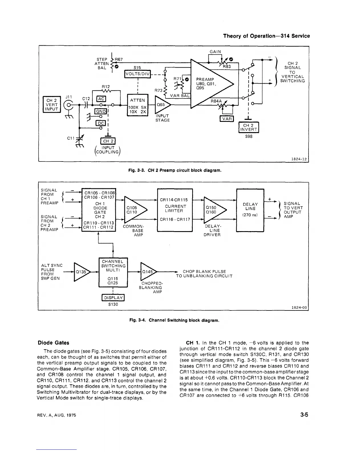
Theory of Operation-314 Service
GAIN
STAGE
S98
Fig. 3-3. CH
2
Preamp circuit block diagram.
SIGNAL
FROM
CH 1
PREAMP
SIGNAL
FROM
CH
2
PREAMP
-
CR105
-
CR108
{T
CR106-CR107
*
CR114-CR115
+
CH 1
CURRENT
DELAY
DIODE
LIMITER
LlNE
GATE
CH
2
(270
ns)
-
*
CR116-CR117
-
CR110-CR113
CR111 -CR112 COW'V'ION-
{--
BASE DELAY- LINE
AMP DRIVER
SIGNAL
TO VERT
OUTPUT
AMP
CHANNEL
ALT SYNC SWITCHING
PULSE
MULTI
FROM
CHOP BLANK PULSE
SWP GEN
TO
UNBLANKING CIRCUIT
BLANKING
AMP
-
-- -
--
Fig.
3-4.
Channel Switching block diagram.
Diode Gates
CH
1.
In the CH 1 mode, -6 volts is applied to the
The diode gates (see Fig. 3-5) consisting of four diodes
junction of
CR111-CR112 in the channel 2 diode gate
each, can be thought of as switches that permit either of
through vertical mode switch S130C, R131, and CR130
the vertical preamp output signals to be coupled to the
(see simplified diagram, Fig. 3-5). This -6 volts forward
biases CR111 and CR112 and reverse biases CR110 and
Common-Base Amplifier stage. CR105, CR106, CR107,
CR113 since the input to the common-base amplifier stage
and CR108 control the channel 1 signal output, and
is at about +0.6 volts. CR11O-CR113 block the Channel 2
CR1
lo'
CR1
11' CR112'
and CR113
the
channel
signal so it cannot passtothe Common-Base Amplifier, At
signal output. These diodes are, in turn, controlled by the
Switching Multivibrator for dual-trace displays, or by the
the same time, in the Channel 1 Diode Gate, CR106 and
Vertical Mode switch for single-trace displays.
CR107 are connected to t6 volts through R115. CR1 06
REV. A, AUG. 1975
3-5