TM 11-6625-2735-14-1
Section 3—475 Service
CIRCUIT DESCRIPTION
Introduction
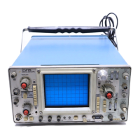
This section of the manual describes the circuitry used
in the 475 Oscilloscope. The description begins with a
discussion of the instrument, using a basic block diagram.
Next, each circuit is described in detail, using detailed
block diagrams
when appropriate, to show the
relationships between the stages in each major circuit.
Digital Logic
Digital logic techniques are used to perform many
functions within this instrument. The function and opera-
tion of the logic circuits are described using logic
symbology and terminology. All logic functions are
described using the positive logic convention. Positive
logic is a system of notation where the more positive of
two levels (HI) is called the true or 1 state; the more
negative level (LO) is called the false or 0 state. The HI-LO
method of notation is used in this logic description. The
specific voltages that constitute a HI or LO state vary
between individual devices.
NOTE
The HI-LO logic notation can be conveniently converted
to 1-0 notation by disregarding the first letter of each step.
Thus:
Hl=1
LO=0
It should be noted that not all of the integrated circuit
devices in this instrument are digital logic devices. The
function of non-digital devices are described individually,
using operating waveforms or other techniques to il-
lustrate their function.
OUTLINE FOR CIRCUIT DESCRIPTION
BLOCK DIAGRAM
General
Page 3-2
CHANNEL 1 PREAMP
General
Page 3-4
Input Coupling
Page 3-5
Input Attenuator
Page 3-5
First Cascode Amplifier
Page 3-5
Second Cascode Amplifier
Page 3-6
Third Cascode Amplifier
Page 3-6
CHANNEL 2 PREAMP
General
First Cascode Amplifier
VERTICAL CHANNEL SWITCHING
General
Channel Switch IC
Switching Logic Flip-Flops
Two Megahertz Clock
Chop Blanking Amplifier
Channel 2 Signal Output Amplifier
Normal Trigger Pickoff Amplifier
Scale-Factor Switching Circuits
VERTICAL OUTPUT AMPLIFIER
General
First IC Amplifier
Second IC Amplifier
A
B
TRIGGER GENERATOR
General
Trigger Source
Trigger Coupling
Input Source Follower
Paraphase Amplifier
Tunnel Diode Driver
Trigger View Amplifier
TRIGGER GENERATOR
General
Trigger Source
SWEEP AND Z-AXIS LOGIC
General
Sweep Control Integrated Circuit
Main Gate Comparator
Delayed Gate Comparator
A Trigger TD Reset Circuit
Holdoff Start Circuit
Z Axis Logic Multivibrator
Delaying Sweep Latch Circuit
B Trigger TD Reset Circuit
Main Sweep Holdoff Gate and
Delayed Sweep Override Amplifier
A +GATE And B +GATE Amplifiers
LOWLINE Indicator Circuit
Page 3-6
Page 3-7
Page 3-7
Page 3-8
Page 3-8
Page 3-9
Page 3-9
Page 3-9
Page 3-9
Page 3-9
Page 3-9
Page 3-9
Page 3-10
Page 3-10
Page 3-11
Page 3-11
Page 3-11
Page 3-11
Page 3-11
Page 3-11
Page 3-12
Page 3-12
Page 3-12
Page 3-13
Page 3-14
Page 3-14
Page 3-14
Page 3-14
Page 3-14
Page 3-15
Page 3-15
Page 3-15
Page 3-15
Page 3-15
3-1

 Loading...