ML865G1 HW Design Guide
1VV0301632 Rev. 4 Page 18 of 86 2020-09-23
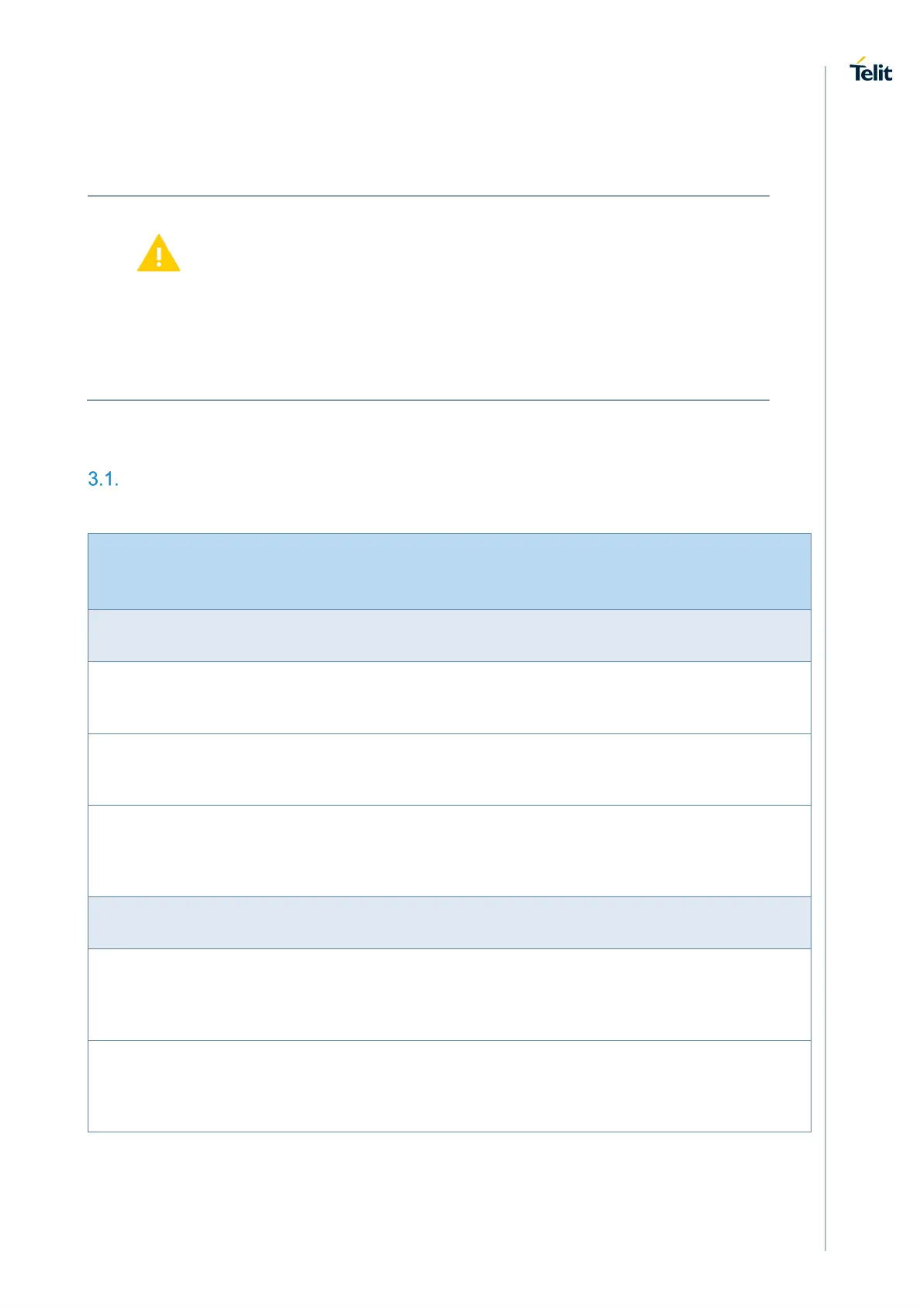
3. PINS ALLOCATION
Warning: ML865G1 is adopting a modified 56-pin xL865 Form Factor,
pin to pin compatible with the previous 48-pin xL865 FF and with 8
additional pads.
The numbering of the pins has been changed accordingly and
attention has to be paid when comparing with previous 48-pin xL865
FF design.
Pin-out
Pin Signal I/
O
Function Type Comment
USB HS 2.0 COMMUNICATION PORT
20 USB_D+ I/O USB differential Data
(+)
3V
19 USB_D- I/O USB differential Data
(-)
3V
18 VUSB I Power sense for the
internal USB
transceiver.
3-5V Internal PD
(100K)
Asynchronous Serial Port (USIF0) - Prog. / Data + HW Flow Control
1 C109/DCD O Output for Data carrier
detect signal (DCD) to
DTE
CMOS
1.8V
2 C125/RING O Output for Ring
indicator signal (RI) to
DTE
CMOS
1.8V