ML865G1 HW Design Guide
1VV0301632 Rev. 4 Page 53 of 86 2020-09-23
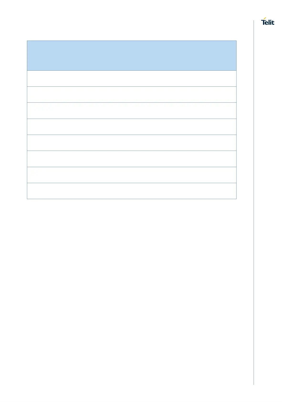
PAD Signal I/O Output
Drive
Strength
Default State NOTE
48 GPIO_01 I/O 1mA
INPUT – PD (100K)
47 GPIO_02 I/O 1mA
INPUT – PD (100K)
46 GPIO_03 I/O 1mA
INPUT – PD (100K)
45 GPIO_04 I/O 1mA
INPUT – PD (100K)
33 GPIO_05 I/O 1mA
INPUT – PD (100K)
32 GPIO_06 I/O 1mA
INPUT – PD (100K)
31 GPIO_07 I/O 1mA
INPUT – PD (100K)
30 GPIO_08 I/O 1mA
INPUT – PD (100K)
5.9.1. Using a GPIO as INPUT
The GPIO pads, when used as inputs, can be connected to a digital output of another
device and report its status, provided this device has interface levels compatible with the
1.8V CMOS levels of the GPIO.
Input current (@1.8V) is about 18uA (corrisponding to 100K pulldown value) in all GPIO
pin. This value is present since ML865 poweron.
If the digital output of the device to be connected with the GPIO input pad has interface
levels different from the 1.8V CMOS, then it can be buffered with an open collector
transistor with a 47K pull up to 1.8V supplied by VAUX/POWERMON (pin 51).