ML865G1 HW Design Guide
1VV0301632 Rev. 4 Page 34 of 86 2020-09-23
5. DIGITAL SECTION
ML865G1 has four main operation states:
• OFF state: Vbatt is applied and only RTC is running. Baseband is switched OFF
and the only change possible is the ON state.
• ON state: baseband is fully switched on and ML865G1 is ready to accept AT
commands. ML865G1 can be idle or connected.
• Sleep mode state: main baseband processor is intermittently switched ON and AT
commands can be processed with some latency. ML865G1 is idle with low current
consumption.
• Deep sleep mode state: PSM defined in 3GPP Release 12. Baseband is switched
OFF most of the time.
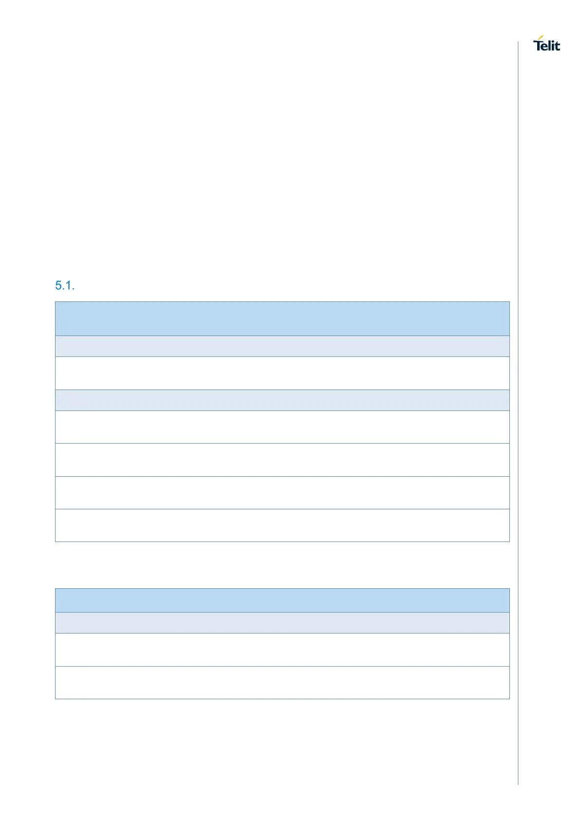
Logic Levels
Parameter Min Max
ABSOLUTE MAXIMUM RATINGS – NOT FUNCTIONAL
Input level on any digital pin (CMOS 1.8) with respect to ground -0.3V 2.1V
Operating Range - Interface levels (1.8V CMOS)
Input high level 1.5V 1.9V
Input low level 0V 0.35V
Output high level 1.6V 1.9V
Output low level 0V 0.2V
Output Current 1mA
Input Current 1uA