ML865G1 HW Design Guide
1VV0301632 Rev. 4 Page 60 of 86 2020-09-23
6.4.2. PCB Guidelines in case of FCC Certification
In the case FCC certification is required for an application using ML865G1, according to
FCC KDB 996369 for modular approval requirements, the transmission line has to be
similar to that implemented on ML865G1 interface board and described in the following
chapter.
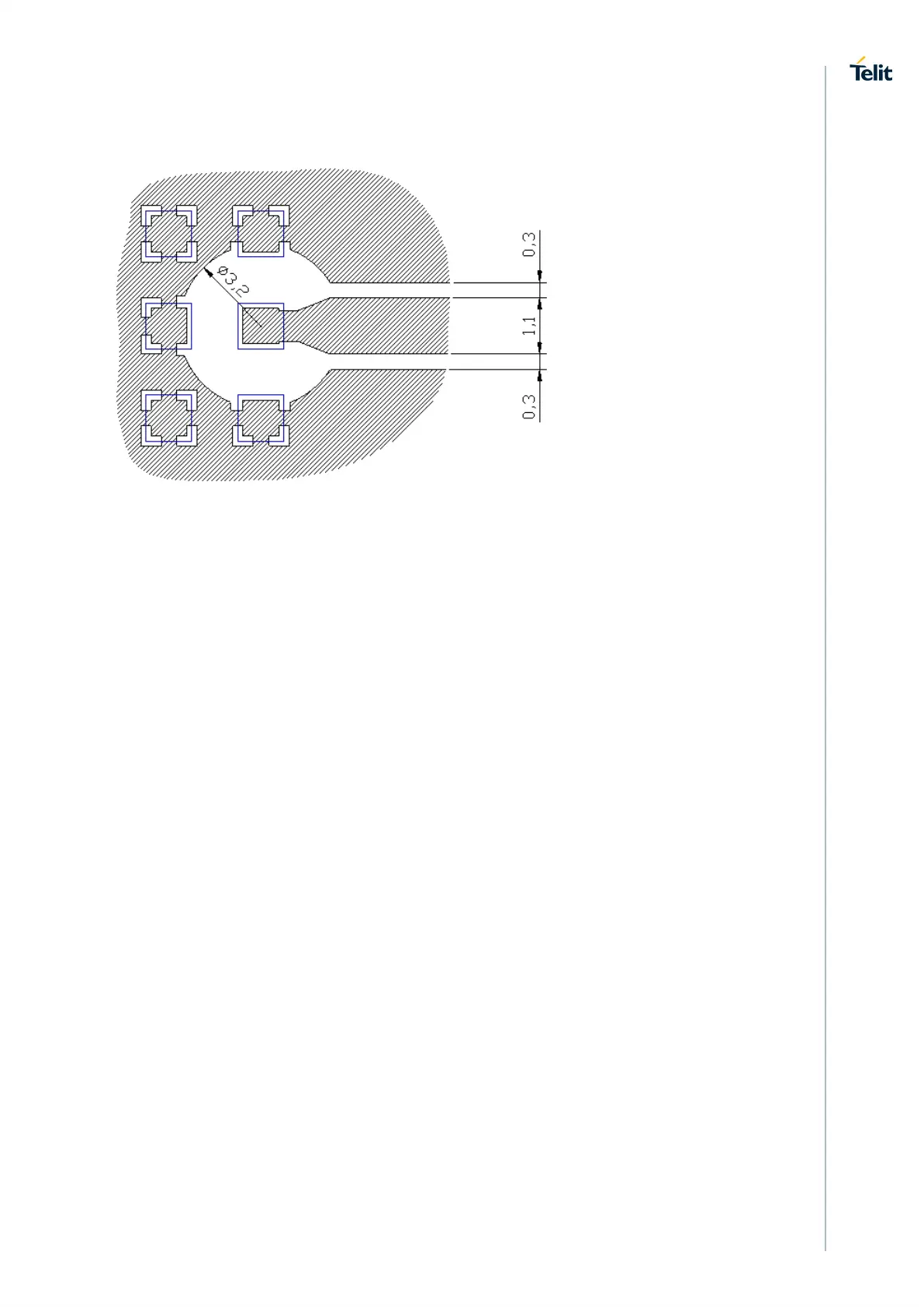
6.4.2.1. Transmission line design
During the design of the ML865G1 interface board, the placement of components has
been chosen properly, in order to keep the line length as short as possible, thus leading to
lowest power losses possible. A Grounded Coplanar Waveguide (G-CPW) line has been
chosen, since this kind of transmission line ensures good impedance control and can be
implemented in an outer PCB layer as needed in this case. A SMA female connector has
been used to feed the line.
The interface board is realized on a FR4, 4-layers PCB. Substrate material is
characterized by relative permittivity εr = 4.6 ± 0.4 @ 1 GHz, TanD= 0.019 ÷ 0.026 @ 1
GHz.