AM3359, AM3358, AM3357, AM3356, AM3354, AM3352
www.ti.com
SPRS717H –OCTOBER 2011–REVISED MAY 2015
power supply ramp-up and ramp-down sequences.
(9) This terminal is connected to analog circuits in the respective USB PHY. The circuit sources a known current while measuring the
voltage to determine if the terminal is connected to VSSA_USB with a resistance less than 10 Ω or greater than 100 kΩ. The terminal
should be connected to ground for USB host operation or open-circuit for USB peripheral operation, and should never be connected to
any external voltage source.
(10) Based on JEDEC JESD78D [IC Latch-Up Test].
(11) For tape and reel the storage temperature range is [–10°C; +50°C] with a maximum relative humidity of 70%. TI recommends returning
to ambient room temperature before usage.
Fail-safe IO terminals are designed such they do not have dependencies on the respective IO power supply
voltage. This allows external voltage sources to be connected to these IO terminals when the respective IO
power supplies are turned off. The USB0_VBUS and USB1_VBUS are the only fail-safe IO terminals. All other IO
terminals are not fail-safe and the voltage applied to them should be limited to the value defined by the steady
state max. Voltage at all IO pins parameter in Section 5.1.
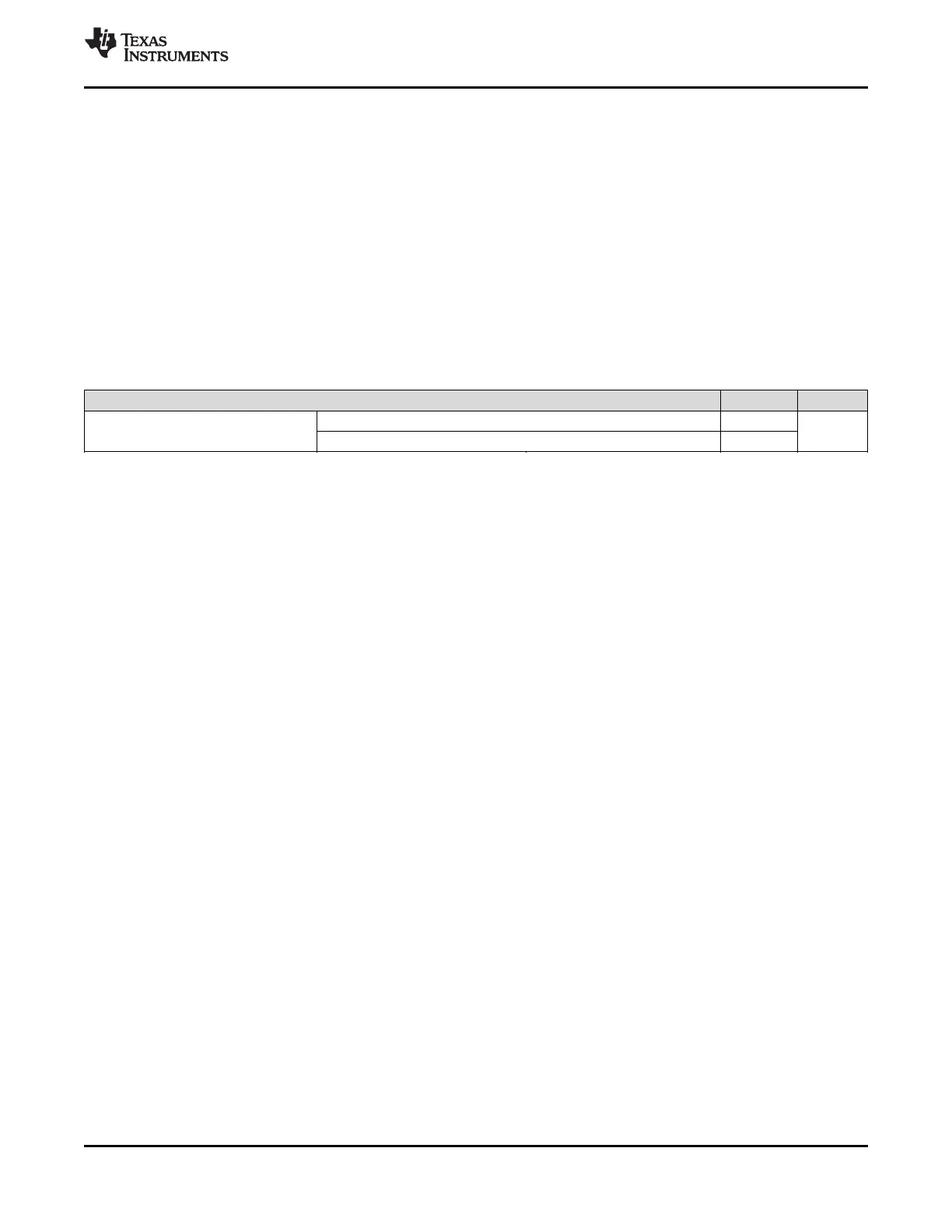
5.2 ESD Ratings
VALUE UNIT
Human Body Model (HBM), per ANSI/ESDA/JEDEC JS001
(1)
±2000
Electrostatic discharge
V
ESD
V
(ESD) performance:
Charged Device Model (CDM), per JESD22-C101
(2)
±500
(1) JEDEC document JEP155 states that 500-V HBM allows safe manufacturing with a standard ESD control process.
(2) JEDEC document JEP157 states that 250-V CDM allows safe manufacturing with a standard ESD control process.
Copyright © 2011–2015, Texas Instruments Incorporated Specifications 81
Submit Documentation Feedback
Product Folder Links: AM3359 AM3358 AM3357 AM3356 AM3354 AM3352
 Loading...