Input Signal-Conditioning Block on the BP-ADS7128
www.ti.com
24
SBAU331–May 2019
Submit Documentation Feedback
Copyright © 2019, Texas Instruments Incorporated
BP-ADS7128 BoosterPack™ Plug-In Module
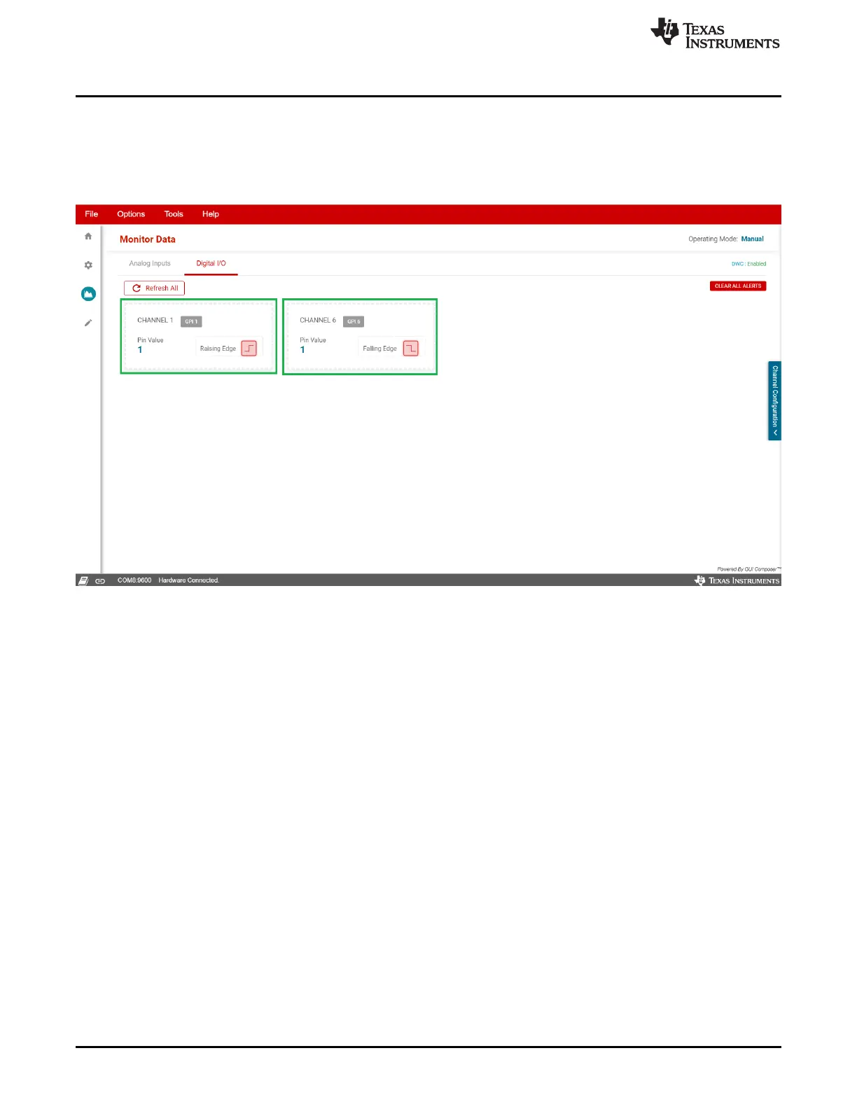
3.3.5.2 Digital I/O Page
The digital I/O page displays the enabled digital input channels as configured in Section 3.3.2.1. In the
example shown in Figure 25, two channels were configured as digital input channels. Each channel
indicates the present logic state, followed by an icon demonstrating the triggering edge for a state change,
rising edge of falling edge. The icon turns red when triggered.
Figure 25. Digital I/O Page Display
4 Input Signal-Conditioning Block on the BP-ADS7128
For applications where the input signal requires additional conditioning before being interfaced to the ADC,
the BP-ADS7128 has an onboard signal-conditioning path on channel 0 between the input signal and the
ADS7128. By default, this signal-conditioning block is populated on the evaluation board as a noninverting
buffer. The board has a provision to bypass the operational amplifier (U4) based on the signal conditioning
requirement. In order to bypass this block, remove the R25 0-Ω resistor and populate R10. See
Section 5.3 for more details.

 Loading...

