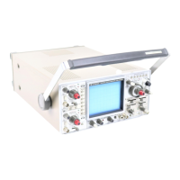
CIRCUIT
DESCRIPTION
VERTICAL ATTENUATOR
The CS-2100A input attenuator consists
of two
stages
of
attenuation having
1/2, 1/4 and 1/10
steps
and the
other
having either
1/10 or 1/100
attenuation
to
form
an
overall
ten point attenuator
in 1-2-5
sequence.
The signal from
the
attenuator
is
passed
to a
dual
FET im-
pedance conversion circuit
(Q1). Its
output
is
sent
to IC12.
Variable gain
is
achieved
by
varying
the
emitter resistance
of
IC12.
The output
of IC12 is
sent
to the
vertical pre-amp.
The arrangement
for CH2 is the
same
as for CH1.
Each channel
has a
50ft termination that
can be
switch
selected.
VERTICAL MODE LOGIC CIRCUIT
Instead
of the
usual mechanical switches used
on
other
instruments
the
CS-2100A makes
use of
electronic switching.
The switches themselves generate
a
single pulse output
when operated
so
that
the
various combinations
of
switches
and holding
of
selected modes must
be
done with external
logic circuitry.
The
circuit that accomplishes this
is the
Ver-
tical Mode Logic Circuit.
The
pulses generated when
the
switches
are
operated
are
shaped
by a
schmitt trigger circuit
and sent
to the
rest
of the
circuitry.
IC6 is a
latch used
to
hold
a
single pulse.
The
input signal, passing through
the
circuit formed
by
D5-D11
and IC3, IC2 and IC7 is a
delayed
pulse which acts
as the
trigger
for IC6. In
this
way IC6
holds
the data that represents
the
fact that
a
switch
has
been
depressed.
IC4
acts
as a
logical single pole double throw
switch
to
select
one of
DUAL/QUAD
and
ALT/CHOP.
CH2
inverter
and
20MHz
BW
switching functions
are
managed
(ON-OFF)
by IC10
which acts
as a
SPST switch.
The
output
of
IC4 is
also latched into
IC6. The
output
of IC6 is
used
to
drive
the
vertical mode LED's through
IC8, IC11, IC5 and
IC9.
VERTICAL PRE-AMP CIRCUIT
The CS-2100A
has
four pre-amp circuits
to
allow 4-channel
operation.
The
output
of the
vertical attenuator
is fed to
IC1,
an amplifier.
For
CH2 an
inverting stage,
IC2, is
provided
to
allow switch-
ed inversion
of
that channel only.
Q2 and Q3
form
the CH1
position circuit.
Q50
and Q51
form
the CH2
position circuit which operates
in
a
similar fashion
to the
circuit
for CH
1.
Q4 and Q5 are x 1
amplifier stages
(for CH1) and Q6, Q7 are x5
amplifier
stages.
The
circuit formed
by Q8 and Q9 is
used
to
switch
between
x 1 and X 5
gain
for
CH1.
For CH2,
Q52/Q53
and
Q54/Q55 along with
Q56 and Q57
have
the
same func-
tions.
Q10/Q11
and
Q19/Q20
for a
cascoded amplifier.
Q18
and Q21 in
combination with
Q19 and Q20
form
a
switching circuit. This circuit
is
used
to
turn
the CH1
signal
on
and off.
Q12
and Q13
form
the
trigger amplifier.
The
trigger signal
passes through
the
buffer output amplifier formed
by Q14
and
Q15,
being converted
to
50ft impedance
and is
sent
to
the
A
trigger switch circuit.
For
channel
1
only,
the
vertical
signal passes through
the
stage formed
by Q16 and Q17 to
the rear panel connector
for CH1
output.
The
circuit
con-
figuration
for CH2, CH3 and CH4 is
similar except that
the
CH3
and CH4
position adjustment
is
accomplished
by
means
of PCB
mounted trimmers
VR1 and VR2.
The
CH1
through
CH4
signals
are
amplified
by the
output
amplifier formed
at the
base side
of the
emitter follower
formed
by Q42 and Q43.
This amplifer consists
of Q44 and
Q45 whose output
is
sent
to the
delay line.
Q38/Q39
and
Q40/Q41
for the
trigger amplifier which
sends
the
signal
of the
output amplifier
to the A
trigger
switch circuit
and
acts
as the V
MODE trigger source.
Q37
acts
as the
load resistance switch
for the ADD
mode.
Q33-
Q36 form
the
20MHz bandwidth circuit which limit
the
ver-
tical bandwidth
to
—
3dB
down
at
20MHz.
CH1 through
CH4
signals
are
switched
by the
logic circuit
formed
by IC3 - IC7 in
accordance with
the
vertical mode
and horizontal mode selected.
VERTICAL OUTPUT AMPLIFIER
The signal from
the
delay line
is
sent
to the
vertical output
amplifier.
Q1, Q2, Q3 and Q4
form
a
cascoded differential
input amplifier.
Q11
forms
a
bias current stabilization circuit
which
in
conjuction with
Q12
forms
the
beam finder circuit.
Q7 —
Q10
form
the
final output stage.
Q5 forms
the
trace separation circuit.
A TRIGGER SWITCH CIRCUIT
The CH1-CH4,
V
MODE signals
are
sent
to the A
trigger
switch circuit.
S1 is the
trigger source switch with
S2 ac-
ting
as the
trigger coupling selection switch.
Q1 and Q2
form
the FIX
synchronization circuit, which detects
the
peak
value
of the
signal
and
acts
as an
automatic trigger level
control.
Q3
and Q4
form
the
VIDEO sync circuit which detects
the
trigger signal
of the TV
picture signal
for
stable display.
Q6
and Q7
form
an
impedance converting emitter follower
circuit
to
lower
the
output impedance
to
drive
the
next
stage.
Q8 and Q9
form
a
circuit which
is
used
to
improve
the CMRR. This circuit
is a
feedback amplifier.
IC1 is a
cascode amplifier used
as the
polarity reversal (inversion)
circuit
for the
trigger signal.
Q10
forms
an
impedance
con-
version stage used
to
convert
the
output
of the IC1
stage
to
50ft
for
output
to the
horizontal sweep unit.
B TRIGGER SWITCH CIRCUIT
Basically this circuit operates
as
does
the A
trigger switch
circuit.
Q1
accepts
the CH2
trigger input
and
uses this
signal
to
form
the X
signal
for X-Y
operation. Other aspects
of operation
are the
same
as the A
trigger switch circuit.
7-1