AC701 Evaluation Board www.xilinx.com 21
UG952 (v1.3) April 7, 2015
Feature Descriptions
SD Card Interface
[Figure 1-2, callout 4]
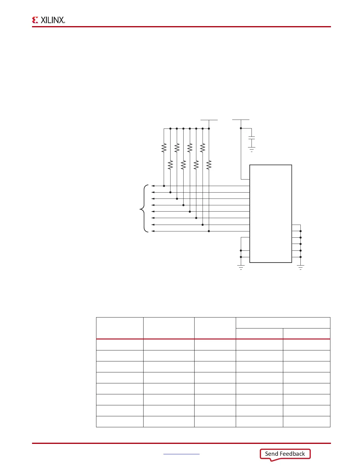
The AC701 board includes a secure digital input/output (SDIO) interface to provide
user-logic access to general purpose nonvolatile SDIO memory cards and peripherals. The
SD card slot is designed to support 50
MHz high speed SD cards.
The SDIO signals are connected to I/O bank 14, which has its VCCO set to 3.3V. Figure 1-7
shows the connections of the SD card interface on the AC701 board.
Table 1-7 lists the SD card interface connections to the FPGA.
X-Ref Target - Figure 1-7
Figure 1-7: SD Card Interface
Table 1-7: SDIO Connections to the FPGA
FPGA Pin (U1)
Schematic Net
Name
I/O Standard
U29 SDIO Connector
Pin Number Pin Name
R20 SDIO_SDWP LVCMOS33 11 SDWP
P24 SDIO_SDDET LVCMOS33 10 SDDET
N23 SDIO_CMD LVCMOS33 2 CMD
N24 SDIO_CLK LVCMOS33 5 CLK
P23 SDIO_DAT2 LVCMOS33 9 DAT2
N19 SDIO_DAT1 LVCMOS33 8 DAT1
P19 SDIO_DAT0 LVCMOS33 7 DAT0
P21 SDIO_CD_DAT3 LVCMOS33 1 CD_DAT3
UG952_c1_07_100212
SDIO Card
Connector
U29
DETECT
DAT2
DAT1
DAT0
CLK
CMD
CD_DAT3
VDD
PROTECT
GNDTAB2VSS1
GNDTAB1
VSS2
GND
GND
SDIO_SDWP
11
SDIO_SDDET
10
SDIO_DAT2
9
SDIO_DAT1
8
SDIO_DAT0 7
SDIO_CLK
5
SDIO_CMD
1SDIO_CD_DAT3
VCC3V3
C52
0.1μF 25V
X5R
GND
4
6
3
D_P
12
GNDTAB3
GNDTAB4
IOGND1
IOGND2
15
16
17
18
13
14
51.1K 1% Eight Places
VCC3V3
R319
R325
R324
R318
R322
R323
R317
R321
2
To
FPGA
Bank 14
(U1)