Appendix A: Default Switch and Jumper Settings
80 www.xilinx.com AC701 Evaluation Board
UG952 (v1.3) April 7, 2015
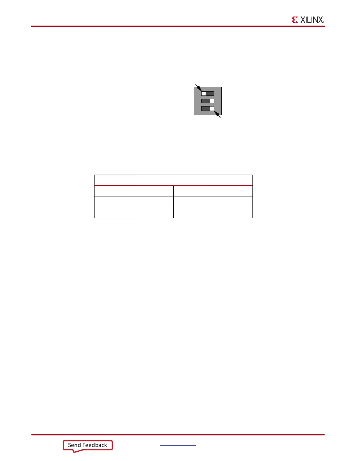
Configuration DIP Switch SW1
See Figure 1-2, page 10 callout 28 for location of SW1. Default settings are shown in
Figure A-2 and details are listed in Table A-2.
The default mode setting M[2:0] = 001 selects Master SPI flash memory configuration at
board power-on.
X-Ref Target - Figure A-2
Figure A-2: SW1 Default Settings
Tabl e A -2 : SW1 Default Switch Settings
Position Function Default
1 FPGA_M2 M2 OFF
2 FPGA_M1 M1 OFF
3 FPGA_M0 M0 ON
UG952_aA_02_011813
SW1 OFF Position = 0
ON Position = 1
1 2 3
M2
M1
M0
ON