66 www.xilinx.com AC701 Evaluation Board
UG952 (v1.3) April 7, 2015
Chapter 1: AC701 Evaluation Board Features
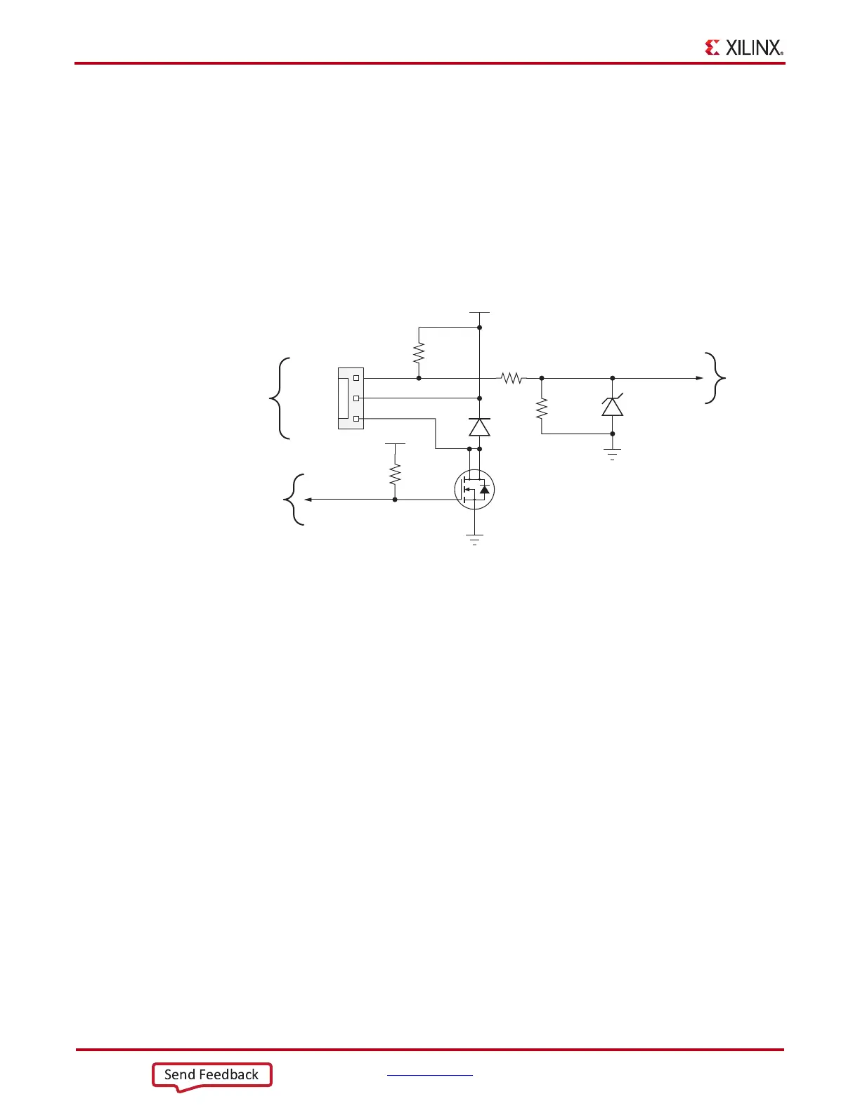
Cooling Fan Control
Cooling fan RPM is controlled and monitored by user-created IP in the FPGA using the fan
control circuit is shown in
Figure 1-43.
FPGA U1 can be cooled by a user-supplied 12V DC fan connected to J61. 12V
DC
is
provided to the fan through J61 pin 2. The fan GND return is provided through J61 pin 1
and transistor Q17. Fan speed is controlled by a pulse-width-modulated signal from FPGA
U1 pin J26 (on Bank 15) driving the gate of Q17. The default unprogrammed FPGA fan
operation mode is ON. The fan speed tachometer signal on J61 pin 3 can be monitored on
FPGA U1 pin J25 (on Bank 15).
AC701 Board Power System
The AC701 board hosts a power system based on the Texas Instruments (TI) UCD90120A
power supply sequencer and monitor, and the LMZ31500 and LMZ31700 family voltage
regulators.
UCD90120A Description
The UCD90120A is a 12-rail PMBus/I2C addressable power-supply sequencer and
monitor. The device integrates a 12-bit ADC for monitoring up to 12 power supply voltage
inputs. Twenty-six GPIO pins can be used for power supply enables, power-on reset
signals, external interrupts, cascading, or other system functions. 12 of these pins offer
PWM functionality. Using these pins, the UCD90120A device offers support for margining
and general-purpose PWM functions.
The UCD90120A device is configured by using the PC-based TI Fusion Digital Power
Designer software. This software provides a graphical user interface (GUI) for configuring,
storing, and monitoring power system operating parameters.
LMZ31500 Family Regulator Description
The LMZ31506RUQ (6A) and LMZ31503RUQ (3A) regulators are integrated synchronous
buck switching regulators that combines a DC/DC converter with power MOSFETs, an
inductor, and passives into low profile, BQFN packages. The LMZ3150x devices accept an
X-Ref Target - Figure 1-43
Figure 1-43: FPGA Cooling Fan Circuit
GND
SM_FAN_PWM
SM_FAN_TACH
1
2
3
J61
R245
10.0K 1%
1/10W
GND
R277
1.00K 1%
1/16W
D15
2.7V
500 mW
MM3Z2V7B
R390
4.75K 1%
1/10W
R393
10.0K 1%
1/10W
VCC12_P
D14
100V
500 mW
DL4148
Q17
NDT30555L
1.3 W
1
2
3
4
VCC2V5
UG952_c1_38_100512
Cooling
Fan
FPGA
U1 Pin J26
FPGA
U1 Pin J25
Fan GND
Fan +12V
Fan Tach