12 www.xilinx.com AC701 Evaluation Board
UG952 (v1.3) April 7, 2015
Chapter 1: AC701 Evaluation Board Features
Artix-7 FPGA
[Figure 1-2, callout 1]
The AC701 board is populated with the Artix-7 XC7A200T-2FBG676C FPGA.
For further information on Artix-7 FPGAs, see 7 Series FPGAs Overview (DS180) [Ref 2].
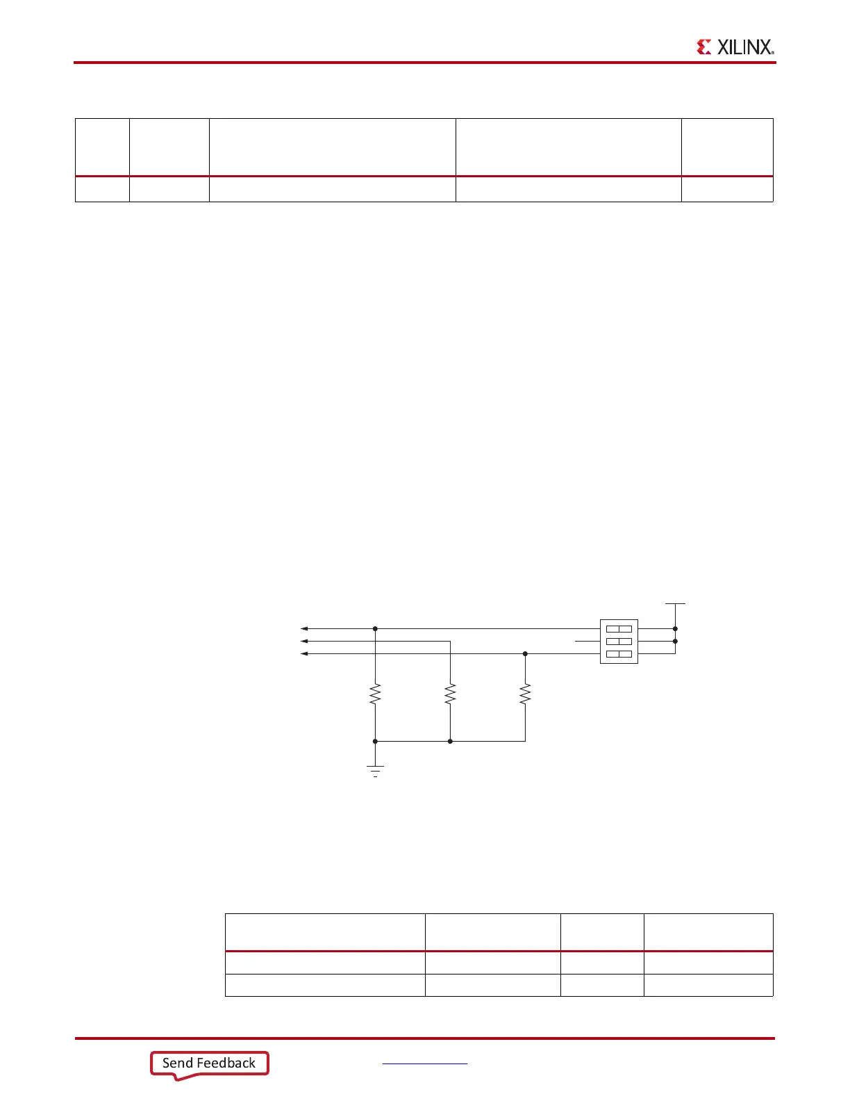
FPGA Configuration
The AC701 board supports two of the five 7 series FPGA configuration modes:
• Master SPI flash memory using the onboard Quad SPI flash memory
• JTAG using a standard-A to micro-B USB cable for connecting the host PC to the
AC701 board configuration port or by J4 Platform Cable USB/Parallel Cable IV flat
cable connector
Each configuration interface corresponds to one or more configuration modes and bus
widths as listed in
Table 1-2. The mode switches M2, M1, and M0 are on SW1 positions 1,
2, and 3 respectively, as shown in Figure 1-3.
The default mode setting is M[2:0] = 001, which selects Master SPI flash memory at board
power-on. See
Configuration Options, page 77 for more information about the mode
switch SW1.
35 U3, U4 GTP transceiver clock multiplexers Micrel SY89544UMG 30
Notes:
1. Jumper header locations are identified in Default Jumper Settings in Appendix A.
Table 1-1: AC701 Board Component Descriptions (Cont’d)
Callout
Reference
Designator
Component Description Notes
Schematic
0381502
Page Number
X-Ref Target - Figure 1-3
Figure 1-3: SW1 Default Settings
Table 1-2: AC701 Board FPGA Configuration Modes
Configuration
Mode
SW1 DIP switch
Settings (M[2:0])
Bus
Width
CCLK
Direction
Master SPI flash memory 001 x1, x2, x4 Output
JTAG 101 x1 Not applicable
R339
1.21K 1%
1/10W
R338
1.21K 1%
1/10W
R337
1.21K 1%
1/10W
FPGA_3V3
SW1
1
2
3
6
5
4
SDA03H1SBD
FPGA_M2
FPGA_M1
FPGA_M0
UG952_c1_03_011713
NC