62 www.xilinx.com AC701 Evaluation Board
UG952 (v1.3) April 7, 2015
Chapter 1: AC701 Evaluation Board Features
The pcb layout and power system design meets the recommended criteria described in the
7
Series FPGAs PCB Design and Pin Planning Guide (UG483) [Ref 11].
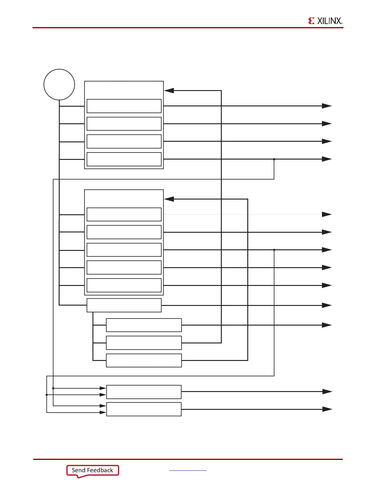
X-Ref Target - Figure 1-42
Figure 1-42: AC701 Board Onboard Power Regulators
UG952_c1_44_030915
VCCAUX
VCCBRAM
FPGA_1V5
VCCO_VADJ
FPGA_1V8
MGTAVCC
12V PWR
Jack
J49
VCC3V3
VCCINT
VCC5V0
VTTDDR
XADC_VCC
DDR3_VTERM
Power Controller 2
PMBUS 102
MGTAVTT
Switching Regulator
5.0V at 4A
U46
Source/Sink Regulator
0.75V at 3A
U37
Source/Sink Regulator
0.75V at 3A
U36
Linear Regulator
1.7V–2.0V at 300 mA
U10
Switching Module
1.5V at 6A
U55
Switching Module
1.0V at 3A
U59
Switching Module
3.3V at 6A
U58
Switching Module
1.8V at 3A
U57
Switching Module
1.2V–3.3V at 6A
U56
Switching Module
1.2V at 3A
U60
Switching Regulator
1.0V at 10A
U49
Switching Module
1.8V at 6A
U53
Switching Module
1.0V at 3A
U54
Power Controller 1
PMBUS 101
U8
U9
1.5V/2=0.75V REFIN
1.5V/2=0.75V REFIN
3.3V POWER
3.3V POWER
V33D_CTL1
Linear Regulator
3.3V at 250 mA
U61
V33D_CTL2
Linear Regulator
3.3V at 250 mA
U63
V33D_CTL2
V33D_CTL1