KCU105 Board User Guide www.xilinx.com 31
UG917 (v1.4) September 25, 2015
Chapter 1: KCU105 Evaluation Board Features
System Clock Source
[Figure 1-2, callout 6]
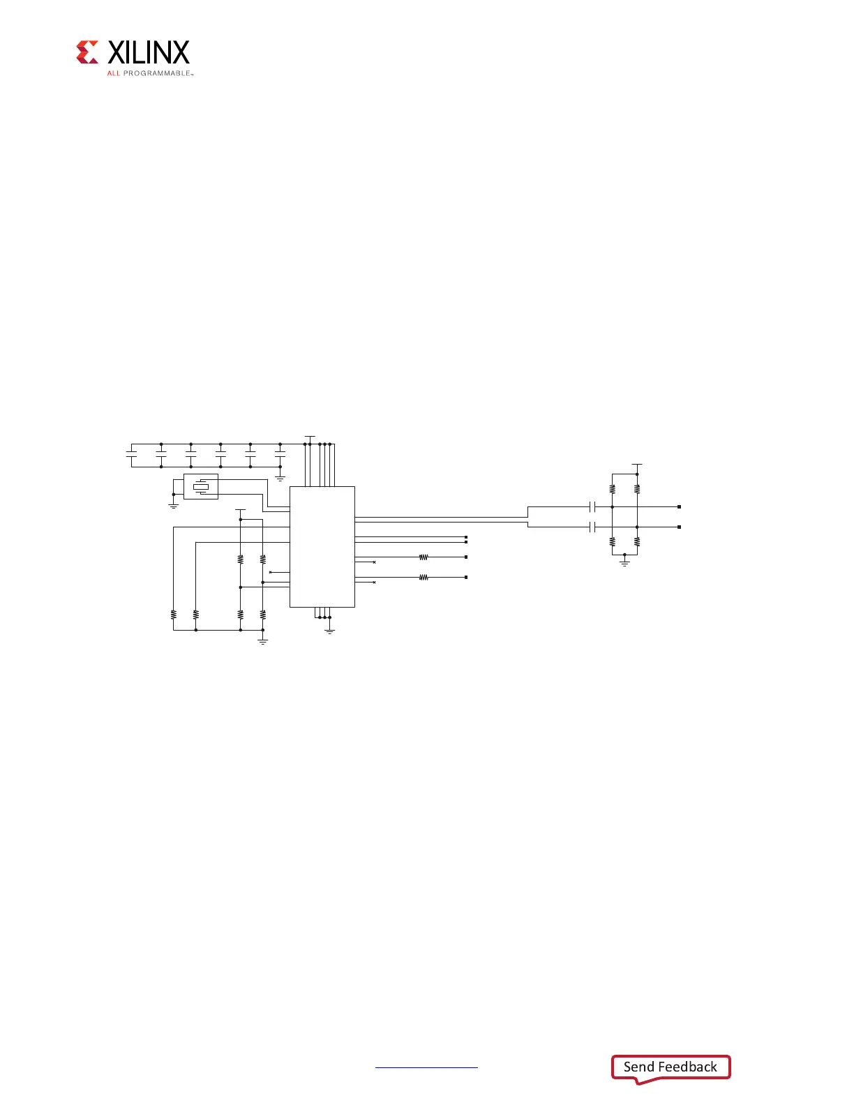
The system clock source is a Silicon Labs Si5335A quad clock generator/buffer at U122. The
system clock (SYSCLK) is a LVDS 300 MHz clock sourced from the CLK0A output pair of
U122. SYSCLK is wired to a clock capable (GC) input on programmable logic bank 45. The
signal pair is named SYSCLK_300_P and SYSCLK_300_N connected to the XCKU040 device
U1 (bank 45 pins AK17 and AK16, respectively).
• Clock Generator: Silicon Labs Si5335A-B03426-GM (CLK0A 300 MHz)
• Low phase jitter of 0.7 pS RMS
• LVDS Differential Output
The system clock circuit is shown in Figure 1-10.
Three additional clocks are sourced from the U122 quad clock generator:
• 125 MHz LVDS signal pair CLK_125MHZ_P and CLK_125MHZ_N, connected to the
XCKU040 device U1 bank 66 pins G10 and F10, respectively.
• 90.0 MHz single-ended 1.8V LVCMOS, series resistor coupled FPGA_EMCCLK,
connected to the XCKU040 device U1 bank 65 dedicated EMCCLK input pin K20.
• 33.3333 MHz single-ended 1.8V LVCMOS, series resistor coupled SYSCTLR_CLK,
connected to system controller XC7Z010 Zynq-7000 AP SoC U111 bank 500 dedicated
PS_CLK input pin C7.
X-Ref Target - Figure 1-10
Figure 1-10: KCU105 Board System Clock
0+]/9&026
5
:
)3*$B(0&&/.B5
)3*$B(0&&/.
0+]/9'6
6<6&/.BB&B1
6<6&/.BB&B3
0+]/9'6
&/.B0+=B1
&/.B
0+=B3
5
.
:
:
.
5
:
.
5
5
.
:
6<6&/.BB1
*1'
9&&9B)3*$
8
;%
5(6(7
2(%B$//
;
$
/26
)6
)6
*1'3$'
*1'
&/.%
&/.%
&/.$
&/.$
&/.%
&/.$
&/.%
&/.$
9''2
9''2
9''2
9''2
9''
9''
*1'
*1'
4)1B;00
6,$%*0
&
8)
9
*1'
*1'
6<6B9
9
8)
&
9
8)
&
&
8)
9
&
8)
9
9
8)
&
*1'
5
'13
'13
'13
'13
'13
'13
5
5
:
:
5
*1'
6<6B9
9
8
)
&
&
8
)
9
6<6&/.BB
3
6<6&7/5B&/.
5
:
1&
1&
6<6&7/5B&/.B5
6<6&/.B2(%B$//
6<6&/.B5(6(7
:
.
5
5
.
:
0+]/9&026
1&
;
;
;
*1'
*1'
0+=
330
8*BB