KCU105 Board User Guide www.xilinx.com 32
UG917 (v1.4) September 25, 2015
Chapter 1: KCU105 Evaluation Board Features
Programmable User Clock Source
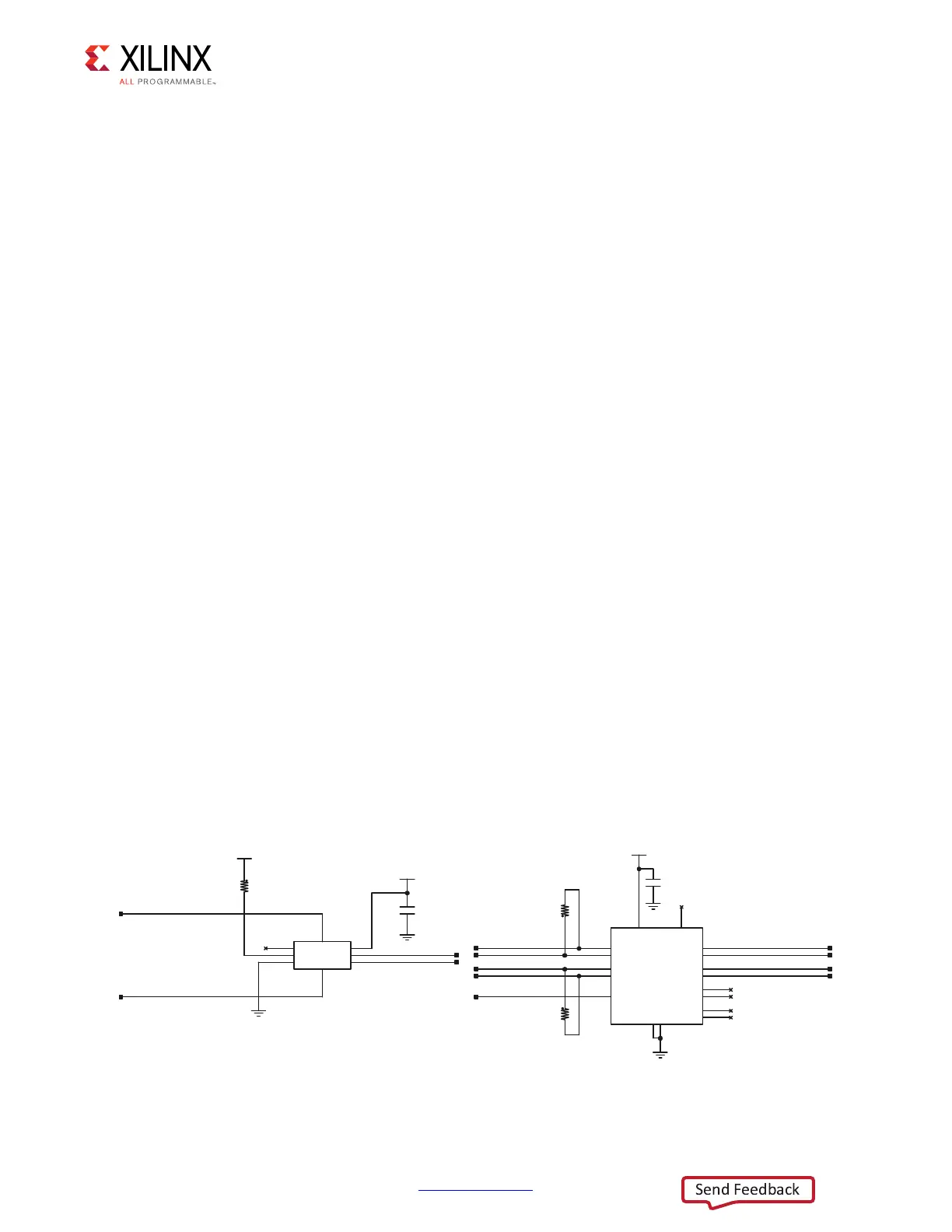
[Figure 1-2, callout 7]
The KCU105 evaluation board has a Si570 programmable low-jitter 3.3V LVDS differential
oscillator (U32) connected to the CLK0 P/N inputs (pin 6 (P) and 7 (N)) of clock buffer
Si53340 U104, a 3.3V 1:4 LOW-JITTER LVDS CLOCK BUFFER WITH 2:1 INPUT MUX.
U104 CLK1 P/N inputs (pin 3 (P) and 4 (N)) are driven from the Si5328B clock multiplier/jitter
attenuator U57 CLKOUT2 pins 35 (P) and 34 (N). The Si5328B is discussed in Jitter
Attenuated Clock.
The 3.3V Si53340 U104 has four LVDS output clock pairs, two (Q2, Q3) unused. U104 output
Q0 drives clock pair USER_SI570_CLOCK_P and USER_SI570_CLOCK_N, connected to the
XCKU040 device U1 bank 65 GC pins M25 and M26, respectively.
U104 output Q1 drives clock pair MGT_SI570_CLOCK_P and MGT_SI570_CLOCK_N, which are
connected to the XCKU040 device U1 GTH BANK 227 MGTREFCLK0P/N pins P6 and P5,
respectively.
The U104 2:1 pin 2
MUX select net SI570_CLK_SEL is connected to the XCKU040 device U1
bank 66 pin G10 via 3.3V-to-1.8V level-shifter U43.
On power-up, the Si570 user clock defaults to an output frequency of 156.250 MHz. User
applications can change the output frequency within the range of 10 MHz to 810 MHz
through an I2C interface. Power cycling the KCU105 evaluation board resets the user clock
to the default frequency of 156.250 MHz.
• Programmable oscillator: Silicon Labs Si570BAB0000544DG (10 MHz-810 MHz)
• Frequency tolerance: 50 ppm
• 3.3V LVDS differential output
The system clock circuit is shown in Figure 1-11.
X-Ref Target - Figure 1-11
Figure 1-11: KCU105 Board User Clock
*1'
*1'
&
8)
9
.
5
86(5B6,B&/2&.B6'$
86(5B6,B&/2&.B6&/
0*7B6,B&/2&.B1
0*7B6,B&/2&.B3
;5
:
1&
86(5B6,B&/2&.B1
86(5B6,B&/2&.B36,B287387B3
6,B287387B1
5
:
9
&
;5
8)
*1'
*1'
1&
1&
1&
1&
1&
6,B287B1
6,B287B3
5
:
6,B&/.B6(/
8
4B3
4B1
&/.B3
&/.B1
&/.B6(/
*1'3$'
*1'
9''
95()
&/.B3
&/.B1
4B3
4B1
4B3
4B1
4B3
4B1
4)1B6,B;00
6,%*0
6,B287387B3
6,B287387B1
8
1&
2(
*1'
6'$
287
287B%
9''
6&/
0+=B72B0+=
330
87,/B9B$
8*BB
87,/B9B$
87,/B9B$