KCU105 Board User Guide www.xilinx.com 33
UG917 (v1.4) September 25, 2015
Chapter 1: KCU105 Evaluation Board Features
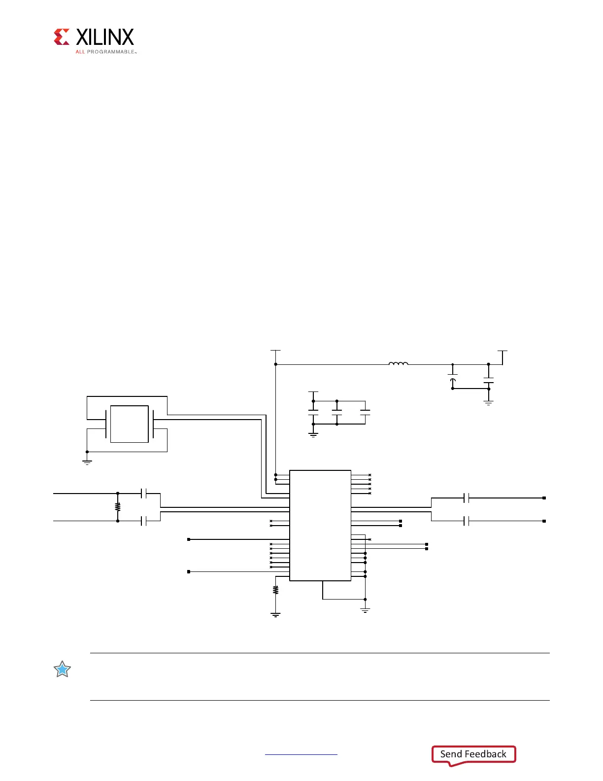
Jitter Attenuated Clock
[Figure 1-2, callout 8]
The KCU105 board includes a Silicon Labs Si5328B jitter attenuator U57 (8 kHz - 808 MHz)
on the back side of the board. The GTH transceiver can output the RX recovered clock to a
differential I/O pair on I/O bank 64 (REC_CLOCK_C_P, pin AG11 and REC_CLOCK_C_N, pin
AH11) for jitter attenuation. The jitter attenuated clock (Si5328_OUT_C_P (U57 pin 28),
Si5328_OUT_C_N (U57 pin 29)) is then routed as a reference clock to GTH Quad 227 inputs
MGTREFCLK0P (U1 pin P6) and MGTREFCLK0N (U1 pin P5).
The primary purpose of this clock is to support synchronous protocols such as CPRI or
OBSAI that perform clock recovery from a user-supplied SFP/SFP+ module and use the jitter
attenuated recovered clock to drive the reference clock inputs of a GTH transceiver. The
system controller configures the Si5328B in free-run mode (see KCU105 Board Zynq-7000
AP SoC XC7Z010 System Controller). Enabling the jitter attenuation feature requires
additional user programming from the FPGA through the I2C bus.
The jitter attenuated clock circuit is shown in Figure 1-12.
IMPORTANT: The Silicon Labs Si5328 U57 pin 1 reset net SI5328_RST must be driven High to enable the
device. U57 pin 1 net SI5328_RST is level-shifted to 1.8V by U47 and is connected to FPGA U1 bank 65
pin K23.
X-Ref Target - Figure 1-12
Figure 1-12: KCU105 Board Jitter Attenuated Clock
*1'
*1'
*1'
*1'
*1'
.
5
6,B9&&
9
8)
&
5
&
8)
9
&
8)
9
6,B9&&
9
8)
&
&
8)
9
9
8)
&
&
8)
9
6,B287B3
5(&B&/2&.B&B1
5(&B&/2&.B&B3
5(&B&/2&.B3
6,B,17B$/0
5(&B&/2&.B1
6,B;7$/B;$
6,B287B1
6,B287B&B3
6,B287B&B1
6,B567
6,B;7$/B;%
6,B6&/
6,B6'$
;
;$ ;%
*1' *1'
0+=
330
;5
:
:
&
8)
9
;5
1&
1&
1&
1&
1&
1&
1&
1&
1&
1&
1&
1&
6,B287B1
6,B287B3
8
$
$B66
&.287B1
&.287B3
&02'(
&6B&$
*1'
*1'
*1'3$'
/2/
1&
1&
1&
6&/
6'$B6'2
9''
567B%
1&
,17B&%
&%
9''
;$
;%
1&9''
5$7(
&.,1B3
&.,1B1
5$7(
&.,1B3
&.,1B1
1&
1&
$
6',
&.287B3
&.287B1
4)1B;00
6,%&*0
1&
1&
87,/B9B$
8*BB
/
)(55,7(
9
8)
&
7$17