KCU105 Board User Guide www.xilinx.com 34
UG917 (v1.4) September 25, 2015
Chapter 1: KCU105 Evaluation Board Features
An active Low input at U57 pin 1 RST_B performs an external hardware reset of this device.
This resets all internal logic to a known state and forces the device registers to their default
value. The clock outputs are disabled during reset. The part must be programmed after a
reset or power on to get a clock output. The reset pin 1 has a weak internal pull-up. For
more details on the Silicon Labs Si5335A, Si570, Si53340, and Si5328B devices, see the
Silicon Labs website [Ref 28]. For more information on UltraScale FPGA clocking, see
UltraScale Architecture Clocking Resources User Guide (UG572) [Ref 5].
User SMA Clock Input
[Figure 1-2, callout 9]
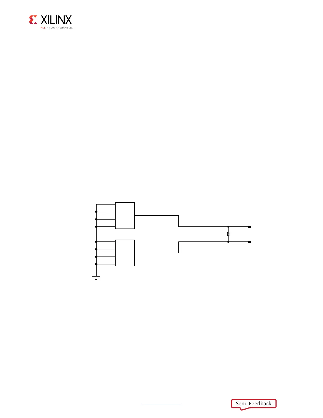
The KCU105 board provides a pair of SMAs for differential user clock input into FPGA U1
bank 67 (see Figure 1-13). The P-side SMA J34 signal USER_SMA_CLOCK_P is connected to
U1 GC pin D23, with the N-side SMA J35 signal USER_SMA_CLOCK_N connected to U1 GC
pin C23. Bank 67 VCCO is nominally 1.8V VADJ_1V8_FPGA. The USER_SMA_CLOCK input
voltage swing should not exceed VADJ. Any signal connected to the USER_SMA_CLOCK
connector inputs must be equal to or less than the VCCO for bank 67. Valid values for the
VADJ rail VADJ_1V8_FPGA are 1.5V and 1.8V. This value must be confirmed prior to applying
signals to the USER_SMA_CLOCK connectors.
X-Ref Target - Figure 1-13
Figure 1-13: User SMA Clock
86(5B60$B&/2&.B3
86(5B60$B&/2&.B1
6,*
*1'
*1'
*1'
*1'
-
6,*
*1'
*1'
*1'
*1'
../
-
*1'
8*BB
5
: