KCU105 Board User Guide www.xilinx.com 35
UG917 (v1.4) September 25, 2015
Chapter 1: KCU105 Evaluation Board Features
GTH SMA Clock Input
[Figure 1-2, callout 10]
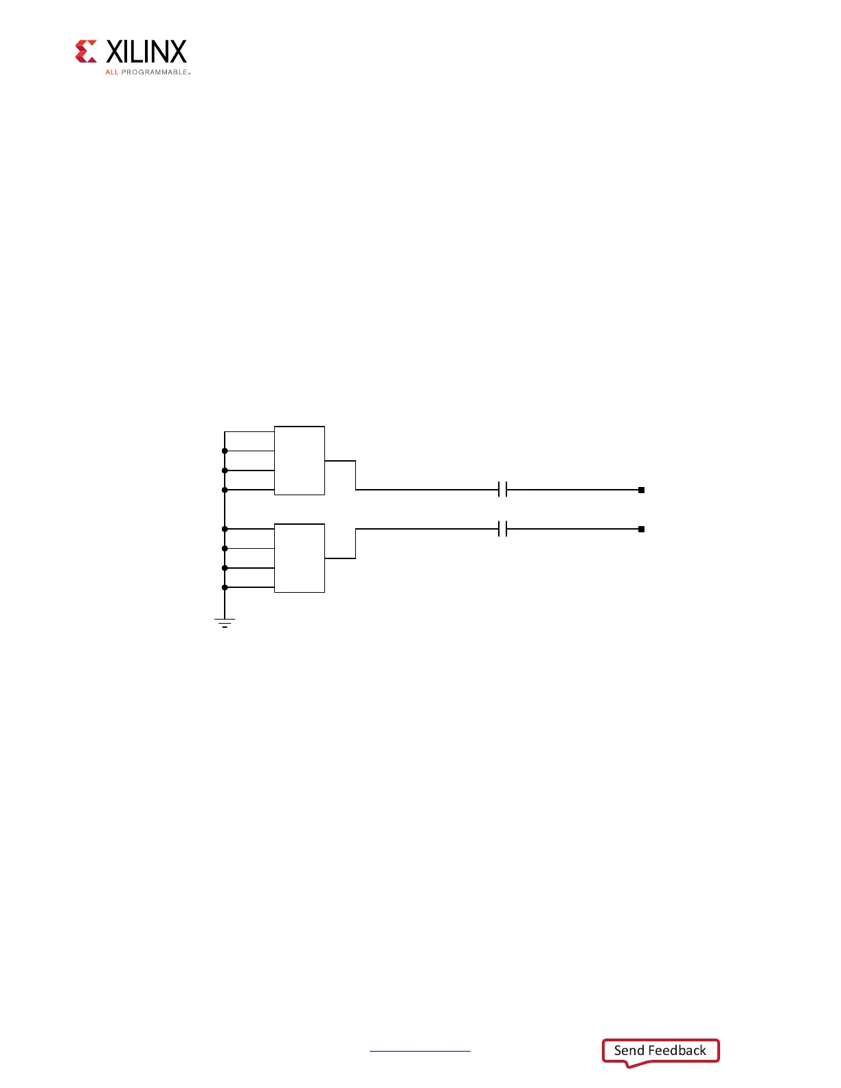
The KCU105 board includes a pair of SMA connectors for a GTH clock wired to GTH Quad
bank 226. This differential clock has signal names SMA_MGT_REFCLK_P and SMA_REFCLK_N,
which are capacitively connected to FPGA U1 GTH bank 226 pins V6 and V5, respectively.
• External user-provided GTH reference clock on SMA input connectors
• Differential Input
The GTH SMA REFCLK signal data paths are routed with a differential characteristic
impedance of 100Ω (±10%).
Figure 1-14 shows this AC-coupled clock circuit.
X-Ref Target - Figure 1-14
Figure 1-14: User GTH REF Clock
60$B0*7B5()&/.B3
60$B0*7B5()&/.B1
6,*
*1'
*1'
*1'
*1'
-
6,*
*1'
*1'
*1'
*1'
../
-
*1'
8*BB
../
9
8)
&
&
8)
9
60$B0*7B5()&/.B&B3
60$B0*7B5()&/.B&B1
SLQ9
SLQ9
WR)3*$8*7+EDQN