KCU105 Board User Guide www.xilinx.com 30
UG917 (v1.4) September 25, 2015
Chapter 1: KCU105 Evaluation Board Features
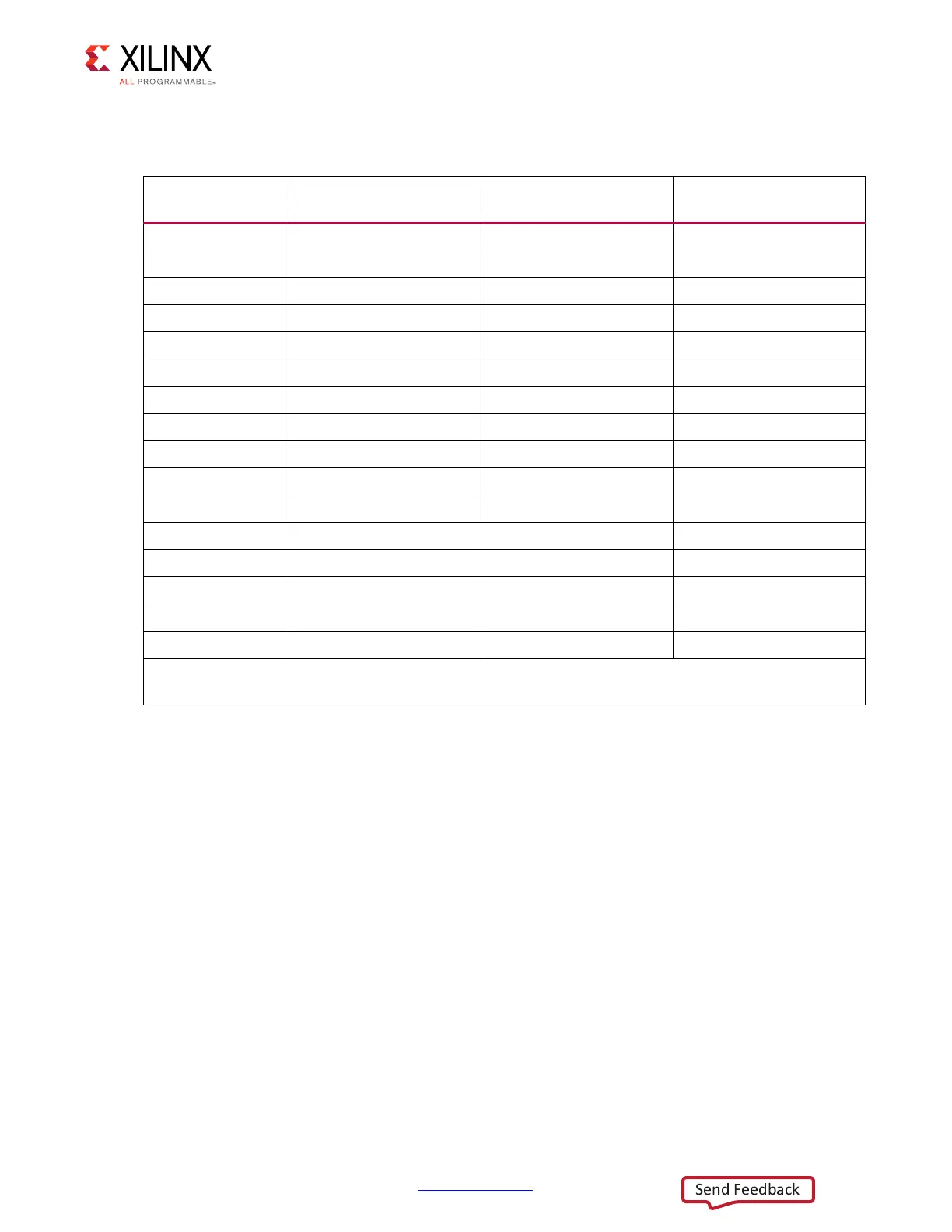
Tab le 1- 8 lists the KCU105 board clock sources to the XCKU040 device U1 connections.
Table 1-8: KCU105 Board Clock Sources to XCKU040 Device U1 Connections
Clock Source Ref.
Des. and Pin
Schematic Net Name I/O Standard XCKU040 Device (U1) Pin
U122.22 SYSCLK_300_P LVDS AK17
U122.21 SYSCLK_300_N LVDS AK16
U122.18 CLK_125MHZ_P LVDS G10
U122.17 CLK_125MHZ_N LVDS F10
U122.14 FPGA_EMCCLK LVCMOS18 K20
U122.10 SYSCTLR_CLK LVCMOS18 C7
U104.9 USER_SI570_CLOCK_P LVDS_25 M25
U104.10 USER_SI570_CLOCK_N LVDS_25 M26
U104.11 MGT_SI570_CLOCK_P NA
(1)
P6
U104.12 MGT_SI570_CLOCK_N NA
(1)
P5
J33.1 SMA_MGT_REFCLK_P NA
(1)
V6
J32.1 SMA_MGT_REFCLK_N NA
(1)
V5
J34.1 USER_SMA_CLOCK_P LVDS D23
J35.1 USER_SMA_CLOCK_N LVDS C23
U57.28 SI5328_OUT_P NA
(1)
M6
U57.29 SI5328_OUT_N NA
(1)
M5
Notes:
1. Capacitively coupled, serial transceiver connections I/O standard not applicable.