KCU105 Board User Guide www.xilinx.com 64
UG917 (v1.4) September 25, 2015
Chapter 1: KCU105 Evaluation Board Features
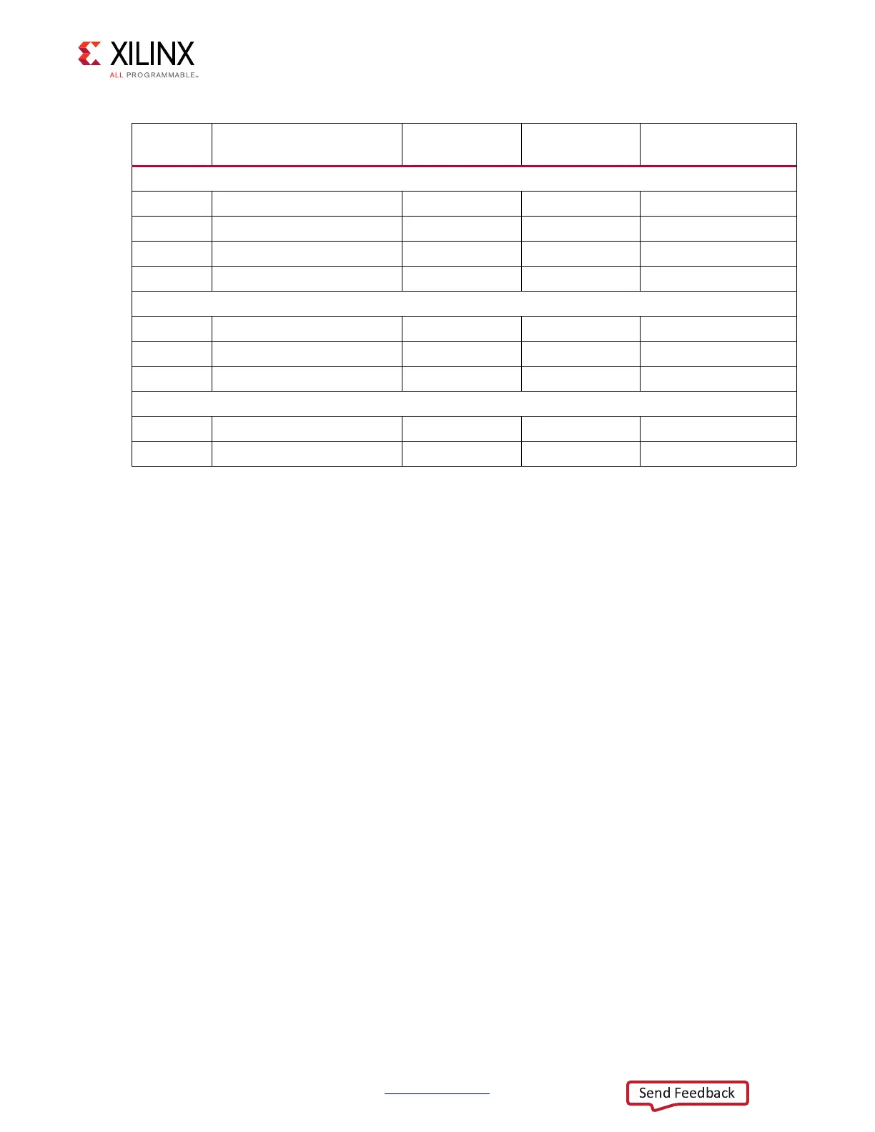
4-Pole DIP SW (Active High)
(1)
AN16 GPIO_DIP_SW0 Input LVCMOS12 SW12.4
AN19 GPIO_DIP_SW1 Input LVCMOS12 SW12.3
AP18 GPIO_DIP_SW2 Input LVCMOS12 SW12.2
AN14 GPIO_DIP_SW3 Input LVCMOS12 SW12.1
User Rotary Switch (Active High)
(1)
Y21 ROTARY_INCA Input LVCMOS18 SW13.1
AD26 ROTARY_INCB Input LVCMOS18 SW13.6
AF28 ROTARY_PUSH Input LVCMOS18 SW13.5
User GPIO SMA
G27 USER_SMA_GPIO_N I/O LVCMOS18 J36.1
H27 USER_SMA_GPIO_P I/O LVCMOS18 J36.1
Notes:
1. Routed through a 3.3V-to-1.8V level-shifter to FPGA.
Table 1-21: KCU105 Board GPIO Connections to FPGA U1 (Cont’d)
FPGA (U1)
Pin
Schematic Net Name
FPGA (U1)
Direction
I/O Standard Device