KCU105 Board User Guide www.xilinx.com 63
UG917 (v1.4) September 25, 2015
Chapter 1: KCU105 Evaluation Board Features
User SMA GPIO
[Figure 1-2, callout 11]
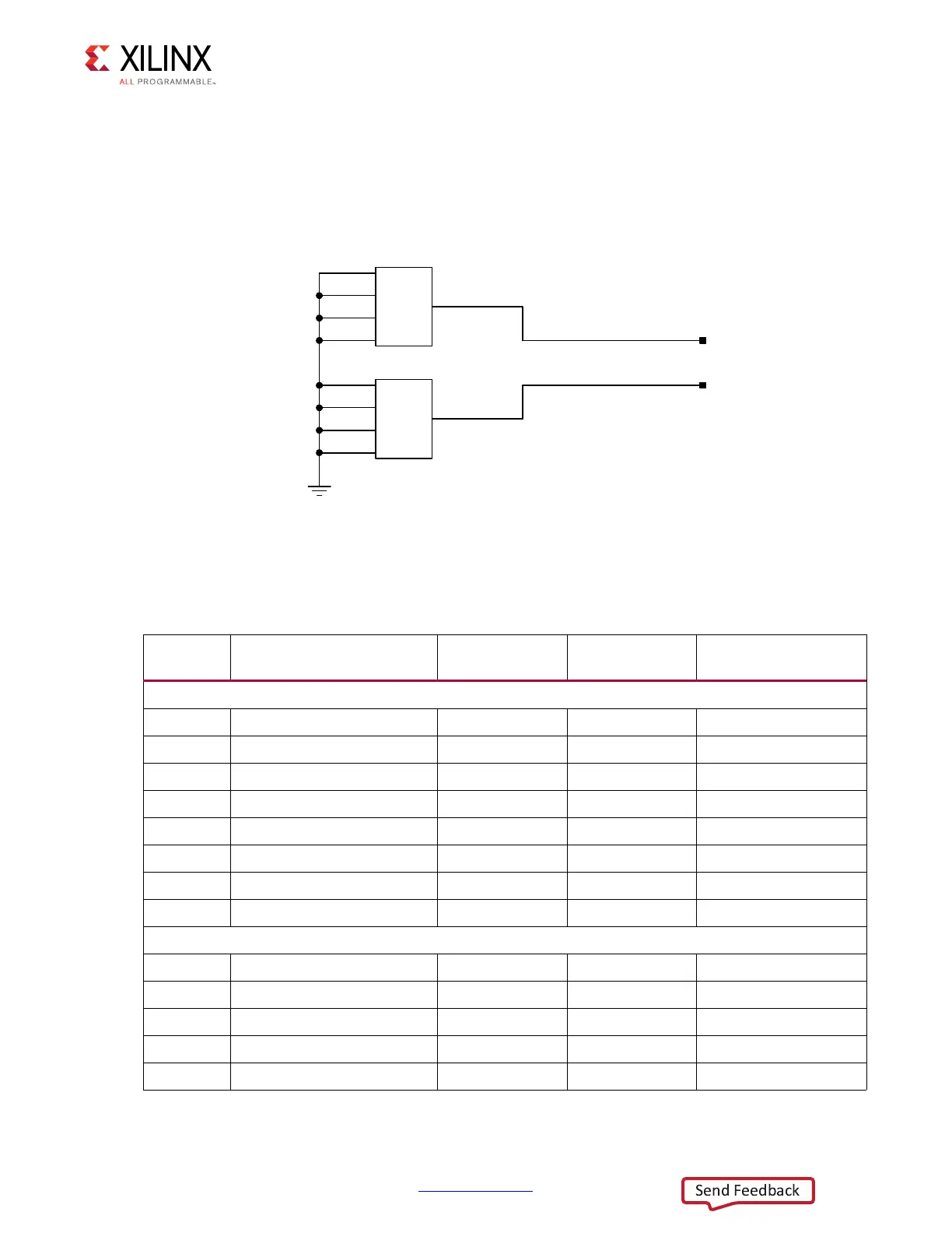
Figure 1-29 shows the GPIO SMAs J36 and J37.
Tab le 1- 21 lists the GPIO Connections to FPGA U1.
X-Ref Target - Figure 1-29
Figure 1-29: GPIO SMAs J36 and J37
Table 1-21: KCU105 Board GPIO Connections to FPGA U1
FPGA (U1)
Pin
Schematic Net Name
FPGA (U1)
Direction
I/O Standard Device
GPIO LEDs (Active High)
(1)
AP8 GPIO_LED_0 Output LVCMOS18 DS7.1
H23 GPIO_LED_1 Output LVCMOS18 DS6.1
P20 GPIO_LED_2 Output LVCMOS18 DS8.1
P21 GPIO_LED_3 Output LVCMOS18 DS9.1
N22 GPIO_LED_4 Output LVCMOS18 DS10.1
M22 GPIO_LED_5 Output LVCMOS18 DS33.1
R23 GPIO_LED_6 Output LVCMOS18 DS32.1
P23 GPIO_LED_7 Output LVCMOS18 DS31.1
Directional Pushbuttons (Active High)
AD10 GPIO_SW_N Input LVCMOS18 SW10.3, U111.A13
AE8 GPIO_SW_E Input LVCMOS18 SW9.3, U111.B14
AF9 GPIO_SW_W Input LVCMOS18 SW6.3, U111.D14
AF8 GPIO_SW_S Input LVCMOS18 SW8.3, U111.C14
AE10 GPIO_SW_C Input LVCMOS18 SW7.3, U111.B12
*1'
86(5B60$B*3,2B3
86(5B60$B*3,2B1
6,*
*1'
*1'
*1'
*1'
-
../
6,*
*1'
*1'
*1'
*1'
../
-
8*BB