26 www.xilinx.com Spartan-6 FPGA Power Management
UG394 (v1.1) September 4, 2012
Chapter 2: Voltage Supplies
V
CCINT
V
CCINT
is the primary power supply for the FPGA. In the Spartan-6 LXT family and the
standard devices in the Spartan-6 LX family (-2 and -3 speed grades), V
CCINT
has a
nominal value of 1.2V. The lower-power Spartan-6 LX devices (-1L speed grade) uses a
nominal V
CCINT
of 1.0V. See Chapter 3, Lower-Power Spartan-6 LX Devices.
V
CCAUX
V
CCAUX
powers the auxiliary logic, including configuration logic and some internal and
I/O resources. The Spartan-6 FPGA’s V
CCAUX
is either 2.5V or 3.3V. These two voltages
provide greater flexibility and allow V
CCAUX
to be set to the same level as an existing V
CCO
rail, to minimize the number of power rails. Reducing V
CCAUX
to 2.5V can reduce the
power consumption on the V
CCAUX
rail by 40%.
During configuration, if V
CCO_2
is 1.8V, V
CCAUX
must be 2.5V. If V
CCO_2
is 2.5V or 3.3V,
V
CCAUX
can be either 2.5V or 3.3V. See UG380, Spartan-6 FPGA Configuration User Guide.
The -1L speed grade devices require V
CCAUX
= 2.5V when using the LVDS_25, LVDS_33,
BLVDS_25, LVPECL_25, RSDS_25, RSDS_33, PPDS_25, and PPDS_33 I/O standards on
inputs. See DS162
, Spartan-6 FPGA Data Sheet: DC and Switching Characteristics.
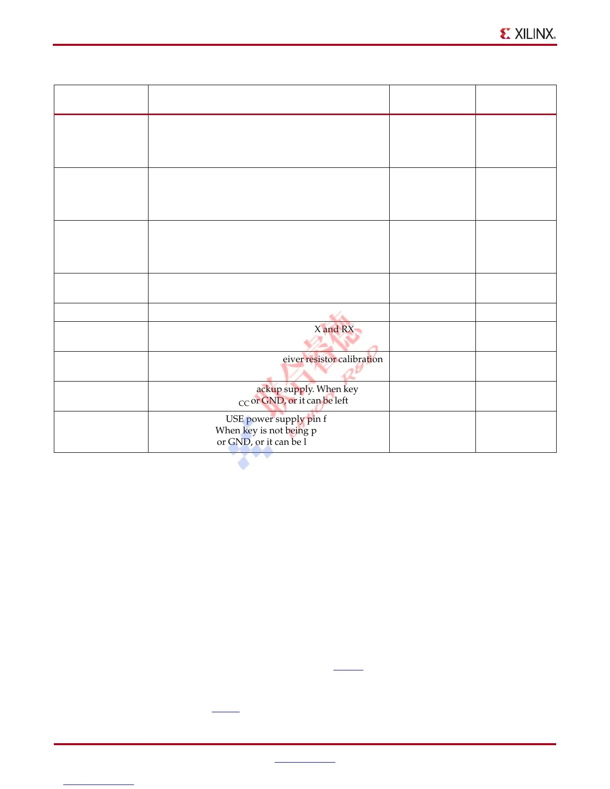
V
CCO_4
Supplies the output buffers in I/O bank 4, the bank
along the top of the left edge of the FPGA in 6-bank
devices.
LX75/T, LX100/T,
and the LX150/T
in FG(G)676 and
FG(G)900
Selectable: 3.3V,
2.5V, 1.8V, 1.5V,
or 1.2V
V
CCO_5
Supplies the output buffers in I/O bank 5, the bank
along the top of the right edge of the FPGA in 6-bank
devices.
LX75/T, LX100/T,
and the LX150/T
in FG(G)676 and
FG(G)900
Selectable: 3.3V,
2.5V, 1.8V, 1.5V,
or 1.2V
V
REF
Input threshold voltage pins when HSTL/SSTL
standards are used in the bank, otherwise user I/Os.
When used as a reference voltage within a bank, all
V
REF
pins within that bank must be connected.
All Varies
MGTAVCC
Power-supply pin for the transceiver mixed-signal
circuitry.
LXT 1.2V
MGTAVCCPLL0/1 Power-supply pin for the transceiver PLL LXT 1.2V
MGTAVTTTX/RX
Power-supply pin for the transceiver TX and RX
circuitry.
LXT 1.2V
MGTAVTTRCAL
Power-supply pin for the transceiver resistor calibration
circuit.
LXT 1.2V
V
BATT
Decryptor key memory backup supply. When key is not
used, tie this pin to V
CC
or GND, or it can be left floating.
LX75/T, LX100/T,
LX150/T
3.3V
V
FS
Decryptor key EFUSE power supply pin for
programming. When key is not being programmed, tie
this pin to V
CC
or GND, or it can be left floating.
LX75/T, LX100/T,
LX150/T
3.3V
Table 2-1: Spartan-6 FPGA Voltage Supplies (Cont’d)
Supply Input Description Devices
Nominal Supply
Voltage

 Loading...


