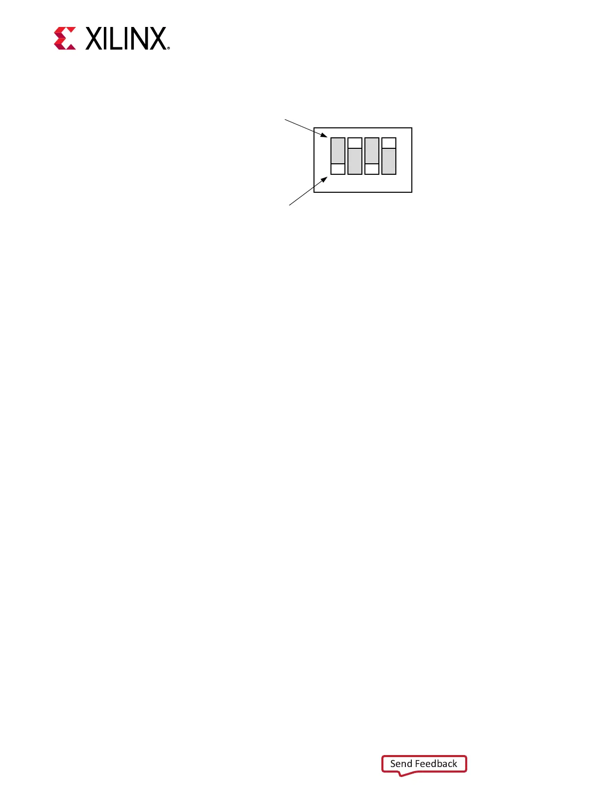
Figure 5: SW1 JTAG Mode Settings
1 2 3 4
SCE
M2
M1
M0
OFF Position = 0
ON Position = 1
SW1
X21648-121918
JTAG
The Vivado
®
, Xilinx
®
SDK, or third-party tools can establish a JTAG connecon to the XCVU37P
FPGA through the FTDI FT4232 USB-to-JTAG/USB UART device (U8) connected to the micro-
USB connector (J2). Alternavely, a JTAG cable can be connected to the keyed at cable header
(J4). JTAG iniated conguraon takes priority over the conguraon method selected through
the FPGA mode pins M[2:0], wired to SW1 posions [2:4].
Quad SPI
To boot from the dual Quad SPI non-volale conguraon memory, follow these steps.
1. Store a valid XCVU37P FPGA boot image in the 2 Gbit Quad SPI ash device (U46)
connected to the FPGA bank 0 Quad SPI interface. See the VCU128 Restoring Flash Tutorial
(XTP533) for informaon on programming the QSPI.
2. Set the boot mode pins SW1 M[2:0] as indicated in the conguraon modes table in FPGA
Conguraon for master SPI.
3. Power-cycle the VCU128 board. Mode SW1 is callout 36 in Figure 2.
See the VCU128 Soware Install and Board Setup Tutorial (XTP535) for more informaon.
See System Controller for an overview of query and control of select programmable board
features such as clocks, FMCP funconality, and power systems. See the VCU128 System
Controller Tutorial (XTP534) for more informaon.
Chapter 2: Board Setup and Configuration
UG1302 (v1.0) December 21, 2018 www.xilinx.com
VCU128 Board User Guide 17