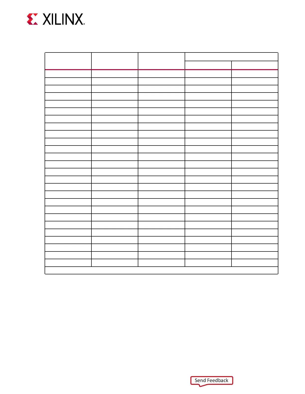
Table 8: QDR4 Memory 72-bit I/F to FPGA U1 Banks 68, 69, and 70 (cont'd)
FPGA (U1) Pin
Schematic Net
Name
I/O Standard
Component Memory
Pin # Pin Name
BF3 QDR4_A8 L13 A8
BG2 QDR4_A9 N7 A9
BG3 QDR4_A10 N13 A10
BG4 QDR4_A11 M8 A11
BG5 QDR4_A12 M12 A12
BF7 QDR4_A13 F8 A13
BF8 QDR4_A14 F12 A14
BG7 QDR4_A15 P8 A15
BG8 QDR4_A16 P12 A16
BJ7 QDR4_A17 L9 A17
BH7 QDR4_A18 L11 A18_36M
BK8 QDR4_A19 J9 A19_72M
BJ8 QDR4_A20 J11 A20_144M
BJ6 QDR4_A21 G9 A21_288M
BK5 QDR4_A22 G11 A22_576M
BH6 QDR4_A23 N9 A23_1152M
BK4 QDR4_A24 N11 A24_2304M
BK6 QDR4_AP P10 AP
BJ1 QDR4_AINV M10 AINV
BH5 QDR4_CK_P J10 CK_P
BH4 QDR4_CK_N K10 CK_N
BJ3 QDR4_LBK0_N A10 LBK0_N
BH1 QDR4_LBK1_N B10 LBK1_N
BH2 QDR4_CFG_N D10 CFG_N
BJ2 QDR4_PE_N V10 PE_N
BK1 QDR4_RST_N K18 RST_N
QDR4 U40 ZQ_ZT pin W10 is wired to 220Ω R604 to GND
Notes:
1. Resistors to GND are 100Ω.
The VCU128 QDR-IV dual independent 36-bit bidireconal data port memory component
interfaces adhere to the constraints guidelines documented in the "QDR-IV Design Guidelines"
secon of the UltraScale Architecture-Based FPGAs Memory IP LogiCORE IP Product Guide (PG150).
The VCU128 QDR-IV memory component interface is a 40Ω impedance implementaon.
For more informaon on the internal VREF, see the "Supply Voltages for the SelectIO Pins",
“VREF”, and “Internal VREF” secons in the UltraScale Architecture SelectIO Resources User Guide
(UG571). For more details about the Cypress QDR-IV component memory, see the Cypress
CY7C4142KV13_106FCXC Data Sheet at the Cypress Semiconductor website.
Chapter 3: Board Component Descriptions
UG1302 (v1.0) December 21, 2018 www.xilinx.com
VCU128 Board User Guide 33