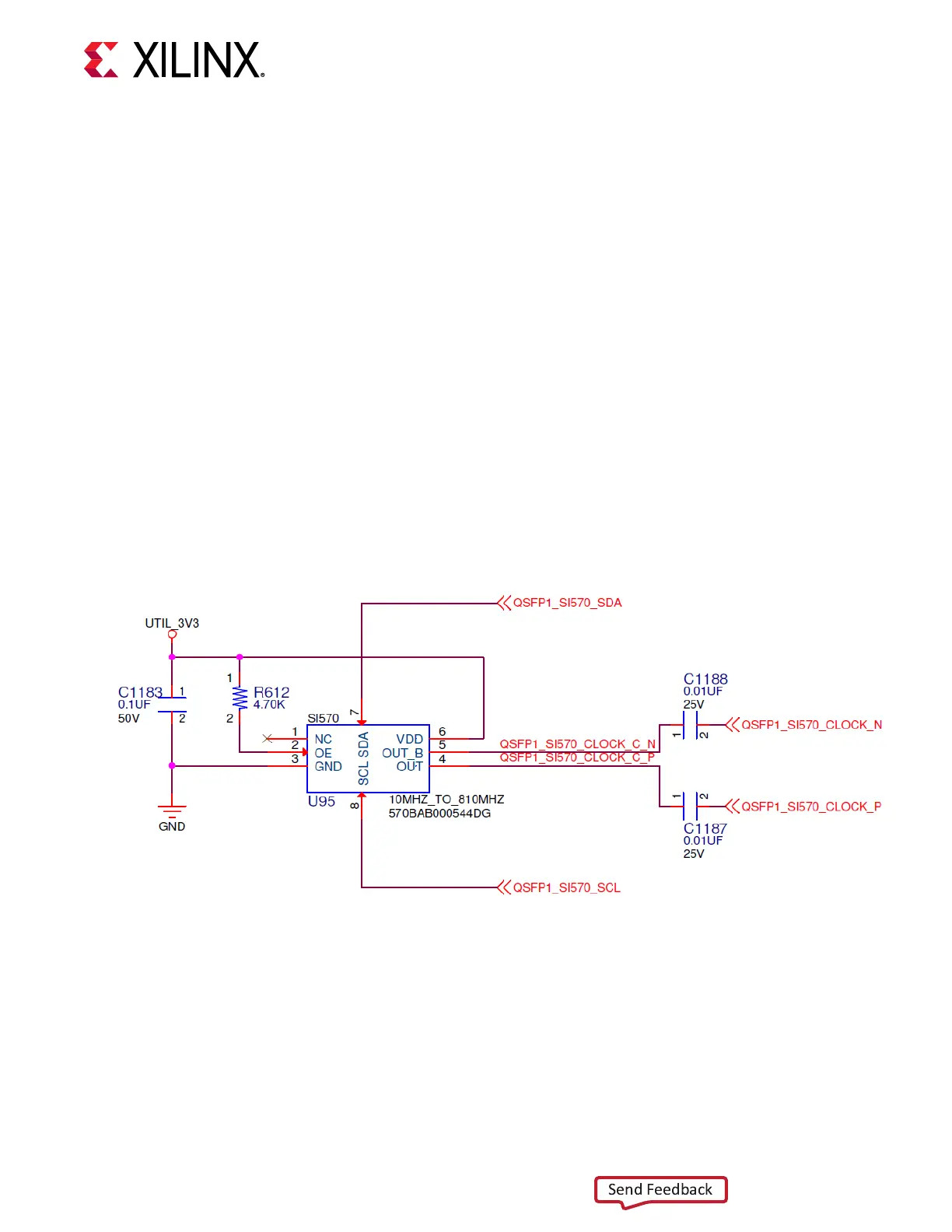
Programmable QSFP1 Clock
[Figure 2, callout 13]
The VCU128 evaluaon board has a SI570 I2C programmable low-jier 3.3V LVDS dierenal
oscillator (U95) connected to FPGA U1 GTY bank 135 MGTREFCLK0 P/N pins P42 and P43
(series capacitor coupled), respecvely.
On power-up, the U95 SI570 user clock defaults to an output frequency of 156.250 MHz. The
Zynq-7000 SoC system controller or FPGA implemented user IP can change the output
frequency within the range of 10 MHz to 810 MHz through an I2C interface. Power cycling the
VCU128 evaluaon board resets the QSFP1 clock to the default frequency of 156.250 MHz.
• Programmable oscillator: Silicon Labs Si570BAB0000544DG (10 MHz-810 MHz)
• Frequency tolerance: 50 ppm
• 3.3V LVDS dierenal output
The programmable QSFP1 clock circuit is shown in the following gure.
Figure 13: QSFP1 Clock
X21963-121918
Chapter 3: Board Component Descriptions
UG1302 (v1.0) December 21, 2018 www.xilinx.com
VCU128 Board User Guide 43