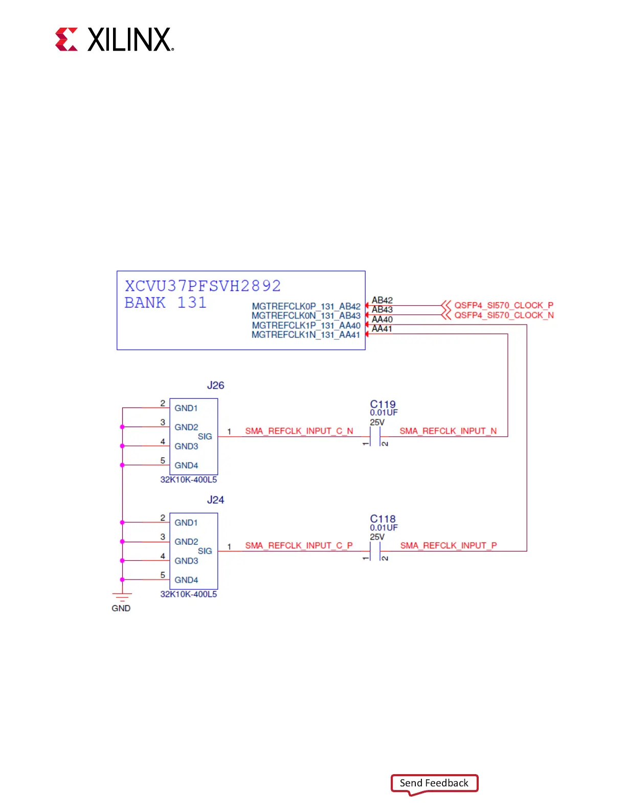
QSFP SMA Clock
[Figure 2, callout 18]
The VCU128 board provides a pair of SMAs for dierenal user clock input into FPGA U1 GTY
bank 131. The P-side SMA J24 signal SMA_REFCLK_INPUT_P is connected to FPGA U1 GTY
bank 131 MGTREFCLK1P pin AA40, with the N-side SMA J26 signal SMA_REFCLK_INPUT_N
connected to U1 GTY bank 131 MGTREFCLK1N pin AA41. The transceiver reference clock pin
absolute input voltage range is –0.5V min. to 1.3V max. The user SMA MGT clock circuit is
shown in the following gure.
Figure 17: QSFP SMA Clock
X21967-121918
Chapter 3: Board Component Descriptions
UG1302 (v1.0) December 21, 2018 www.xilinx.com
VCU128 Board User Guide 47