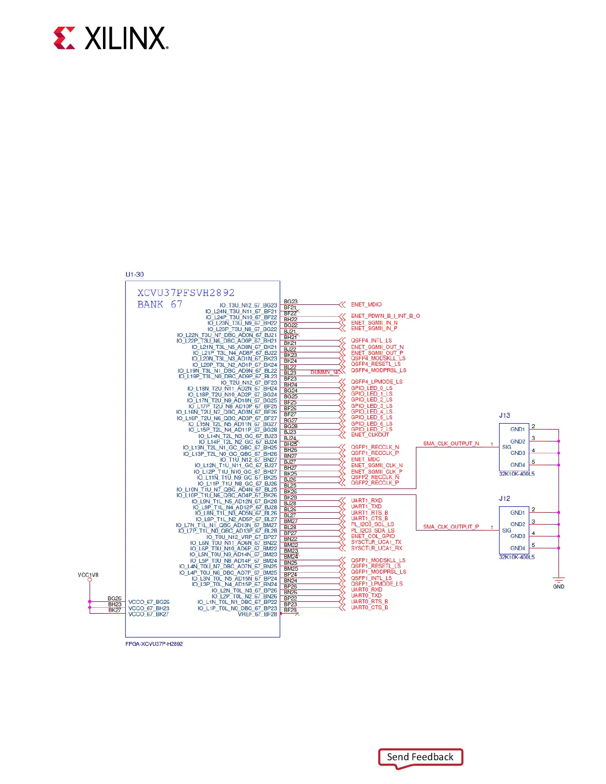
User SMA Clock
[Figure 2, callout 27]
The VCU128 board provides a pair of SMAs for dierenal user clock I/O on FPGA U1 HP bank
67. The P-side SMA J12 net SMA_CLK_OUTPUT_P is connected to FPGA U1 HP bank 67 QBC
pin BK26. The N-side SMA J13 net SMA_CLK_OUTPUT_N is connected to FPGA U1 HP bank
67 QBC pin BL25. Bank 67 VCC1V8 VCCO is nominally 1.8V. Any signal connected to the
SMA_CLK_OUTPUT SMA connectors in input mode must be equal to or less than the VCCO for
bank 67. This value must be conrmed prior to applying signals to the SMA_CLK_OUTPUT
connectors.
Figure 18: User SMA Clock
X22055-121918
Chapter 3: Board Component Descriptions
UG1302 (v1.0) December 21, 2018 www.xilinx.com
VCU128 Board User Guide 48