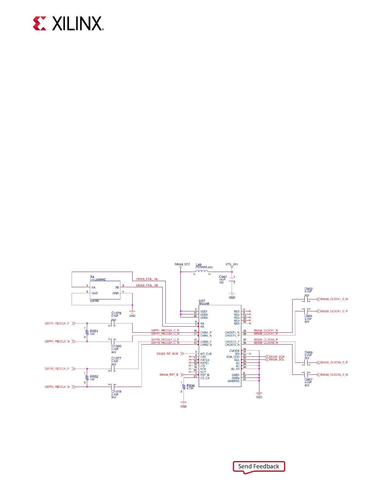
Jitter Attenuated Clock
[Figure 2, callout 17]
The VCU128 board includes a Silicon Labs Si5328B jier aenuator U87 on the back side of the
board. FPGA U1 bank 67 implements two QSFP RX dierenal clocks (QSFP1_RECCLK_P, pin
BH26 and QSFP1_RECCLK_N, pin BH25, and QSFP2_RECCLK_P, pin BJ26 and
QSFP2_RECCLK_N, pin BK25) for jier aenuaon.
The jier aenuated clock pair (SI5328_CLOCK1_C_P (U87 output pin 28),
SI5328_CLOCK1_C_N (U87 output pin 29) is routed as a reference clock to FPGA U1 QSFP2 I/F
GTY Quad 134 inputs MGTREFCLK1P (U1 pin R40) and MGTREFCLK1N (U1 pin R41).
The jier aenuated clock pair (SI5328_CLOCK2_C_P (U87 output pin 35),
SI5328_CLOCK2_C_N (U87 output pin 34) is routed as a reference clock to FPGA U1 QSFP3 I/F
GTY Quad 132 inputs MGTREFCLK1P (U1 pin W40) and MGTREFCLK1N (U1 pin W41).
The primary purpose of this clock is to support synchronous protocols, such as common packet
radio interface (CPRI) or open base staon architecture iniave (OBSAI). These synchronous
protocols perform clock recovery from user-supplied QSFP/QSFP+ modules, and use the jier
aenuated recovered clock to drive the reference clock inputs of a GTY transceiver.
The jier aenuated clock circuit is shown in the following gure.
Figure 19: QSFP Recovery Clock
X21968-121918
Chapter 3: Board Component Descriptions
UG1302 (v1.0) December 21, 2018 www.xilinx.com
VCU128 Board User Guide 49