28 www.xilinx.com VC7203 GTX Transceiver Characterization Board
UG957 (v1.3) October 17, 2014
Chapter 1: VC7203 Board Features and Operation
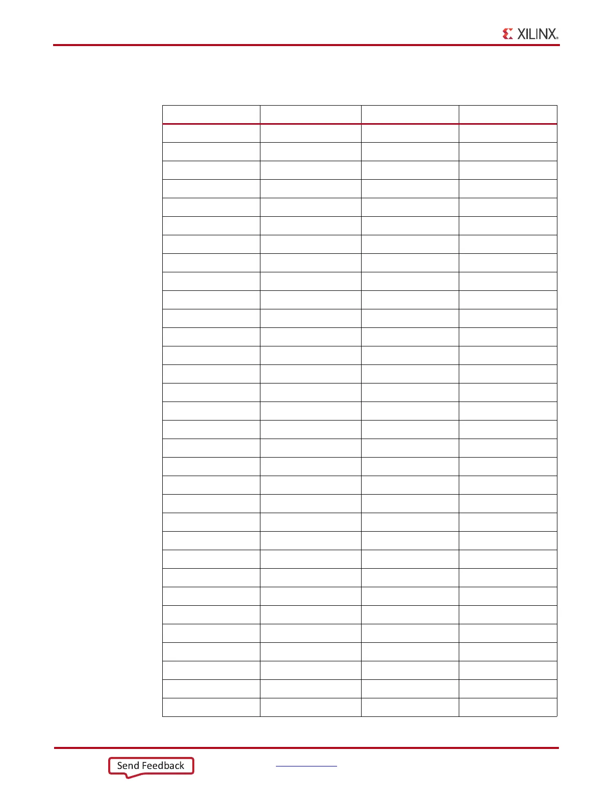
Information for each GTX transceiver clock input is shown in Table 1-14.
Table 1-14: GTX Transceiver Reference Clock Inputs
U1 FPGA Pin Net Name Quad Connector
AW10 111_REFCLK0_P 111 J84
AW9 111_REFCLK0_N 111 J84
BA10 111_REFCLK1_P 111 J84
BA9 111_REFCLK1_N 111 J84
AT8 112_REFCLK0_P 112 J85
AT7 112_REFCLK0_N 112 J85
AU10 112_REFCLK1_P 112 J85
AU9 112_REFCLK1_N 112 J85
AH8 113_REFCLK0_P 113 J86
AH7 113_REFCLK0_N 113 J86
AK7 113_REFCLK1_N 113 J86
AK8 113_REFCLK1_P 113 J86
AD8 114_REFCLK0_P 114 J158
AD7 114_REFCLK0_N 114 J158
AF8 114_REFCLK1_P 114 J158
AF7 114_REFCLK1_N 114 J158
R8 115_REFCLK0_P 115 J83
R7 115_REFCLK0_N 115 J83
U8 115_REFCLK1_P 115 J83
U7 115_REFCLK1_N 115 J83
L8 116_REFCLK0_P 116 J84
L7 116_REFCLK0_N 116 J84
N8 116_REFCLK1_P 116 J84
N7 116_REFCLK1_N 116 J84
G8 117_REFCLK0_P 117 J85
G7 117_REFCLK0_N 117 J85
J8 117_REFCLK1_P 117 J85
J7 117_REFCLK1_N 117 J85
C8 118_REFCLK0_P 118 J86
C7 118_REFCLK0_N 118 J86
E8 118_REFCLK1_P 118 J86
E7 118_REFCLK1_N 118 J86
 Loading...

