ZCU111 Board User Guide 40
UG1271 (v1.1) August 6, 2018 www.xilinx.com
Chapter 3: Board Component Descriptions
The USB3320 is clocked by a 24 MHz crystal (X2). See the Standard Microsystems
Corporation (SMSC) USB3320 data sheet for clocking mode details [Ref 16]. The interface to
the USB3320 PHY is implemented through the IP in the XCZU28DR RFSoC PS.
Tab l e 3- 1 3 describes the jumper settings for the USB 2.0 circuit.
Note:
The bold text in Tabl e 3-1 3 identifies the default shunt positions for USB 2.0 high-speed
on-the-go (OTG) mode.
Note: The shield for the USB 3.0 micro-B connector (J96) can be tied to GND by a jumper on header
J17 pins 2-3 (default). The USB shield can optionally be connected through a series capacitor to GND
by installing a capacitor (body size 0402) at location C171 and jumping pins 1-2 on header J17.
The USB3320 ULPI U12 transceiver circuit (see Figure 3-9) has a Micrel MIC2544 high-side
programmable current limit switch (U13). This switch has an open-drain output fault flag on
pin 2, which turns on LED DS7 if over current or thermal shutdown conditions are detected.
DS7 is located in the U13 circuit area (Figure 2-1, callout 53). Figure 3-9 shows the ULPI U12
transceiver circuit.
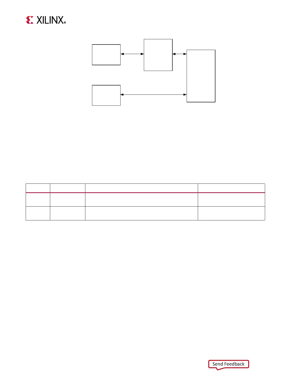
X-Ref Target - Figure 3-8
Figure 3-8: USB Interface
USB
MIO
SM3320
USB2.0
ULPI
USB3
Connector
USB
GTR
GTR Tx, Rx
X20533-062118
Table 3-13: USB Jumper Settings
Header Function Shunt Position Notes
J18 VBUS select
ON = Device mode (150 µF) and VBus power source
OFF = Device mode (5.7 µF)
VBUS load capacitance
J17 Shield select
Position 2-3 = Shield connected to GND
Position 1-2 = Shield floating
Optional C171 in position 1-2