ZCU111 Board User Guide 46
UG1271 (v1.1) August 6, 2018 www.xilinx.com
Chapter 3: Board Component Descriptions
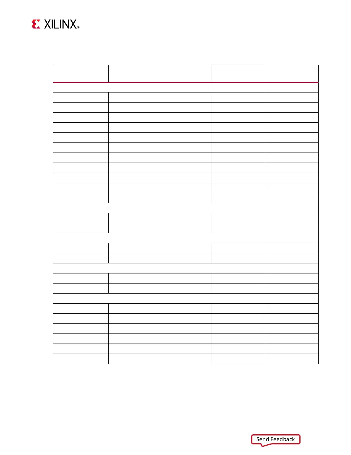
Tab l e 3- 1 7 lists the connections for each clock.
Table 3-17: Clock Connections to XCZU28DR U1
Clock Source Ref.
Des. and Pin
Net Name I/O Standard
XCZU28DR (U1)
Pin
U46 SI5341B Clock Generator
U46.59 PS_REF_CLK (series R310)
(1)
AC30
U46.45 CLK_125_P LVDS AL17
U46.44 CLK_125_N LVDS AM17
U46.42 CLK_100_P LVDS AM15
U46.41 CLK_100_N LVDS AN15
U46.35 GTR_REF_CLK_SATA_P
(2)
AC34
U46.34 GTR_REF_CLK_SATA_N
(2)
AC35
U46.31 GTR_REF_CLK_USB3_P
(2)
AE34
U46.30 GTR_REF_CLK_USB3_N
(2)
AE35
U46.24 GTR_REF_CLK_DP_P
(2)
AG34
U46.23 GTR_REF_CLK_DP_N
(2)
AG35
U47 SI570 I2C Prog. Oscillator (300 MHz default)
U47.4 USER_SI570_P LVDS J19
U47.5 USER_SI570_N LVDS J18
U49 SI570 I2C Prog. Oscillator (156.250 MHz default)
U49.4 USER_MGT_SI570_P
(2)
V31
U49.5 USER_MGT_SI570_N
(2)
V32
J14 (P)/J15 (N) SMA Connectors
J14 USER_SMA_MGT_CLOCK_P
(2)
T31
J15 USER_SMA_MGT_CLOCK_N
(2)
T32
U48 SI5382A Clock Recovery
U48.1 SFP_SI5382_IN1_P
(2)
AA33
U48.2 SFP_SI5382_IN1_N
(2)
AA34
U48.21 SFP_SI5382_OUT_P
(2)
Y31
U48.20 SFP_SI5382_OUT_N
(2)
Y32
U48.63 SFP_REC_CLOCK_P LVDS
(3)
AW14
U48.64 SFP_REC_CLOCK_N LVDS
(3)
AW13
Notes:
1. U1 XCZU28DR bank 503 supports LVCMOS18 level inputs.
2. Series capacitor coupled, U1 MGT (I/O standards do not apply).
3. Series capacitor coupled.