ZCU111 Board User Guide 50
UG1271 (v1.1) August 6, 2018 www.xilinx.com
Chapter 3: Board Component Descriptions
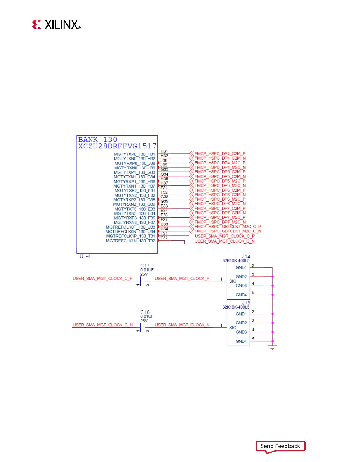
User SMA MGT Clock
[Figure 2-1, callout 48]
The ZCU111 board provides a pair of SMAs for differential AC coupled user MGT clock input
into FPGA U1 GTY bank 130. This differential signal pair is series-capacitor coupled. The
P-side SMA J14 signal USER_SMA_MGT_CLOCK_P is connected to U1 MGTREFCLK1P pin T31,
and the N-side SMA J15 signal USER_SMA_MGT_CLOCK_N is connected to U1
MGTREFCLK1N pin T32. The transceiver reference clock pin absolute input voltage range is
–0.5V min. to 1.3V max. The user SMA MGT clock circuit is shown in Figure 3-16.
X-Ref Target - Figure 3-16
Figure 3-16: User SMA MGT Clock