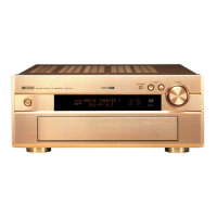
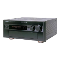
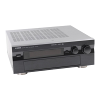
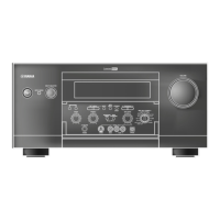
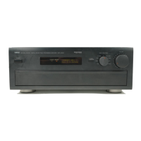
RX-V2500/DSP-AX2500
47
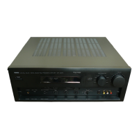
IC512: D601A003BPYP225 (DSP P.C.B)
Decoder
Pin Multiplexing
EMIF32
L1P Cache
Direct Mapped
4K Bytes Total
Digital Signal Processors
L1D Cache
2-Way Set
Associative
4K Bytes Total
Clock Generator,
Oscillator and PLL
x4 through x25 Multipliers
/1 through /32 Dividers
Power-Down
Logic
Instruction Fetch
Instruction Dispatch
Instruction Decode
Data Path BData Path A
B Register File
Control
Registers
C67x
TM
CPU
Control
Logic
In-Circuit
Emulation
Interrupt
Control
Test
A Register File
.L1t
McASP1
McASP0
McBSP1
McBSP0
I2C1
I2C0
Timer 1
Timer 0
.S1t .M1t .D1 .D2 .M2t .S2t .L2t
GP1
GP0
HPI16
Enhanced
DMA
Controller
(16 channel)
L2 Cache/
Memory
4 Banks
64K Bytes
To ta l
(4-Way)
L2
Memory
DA610:
192K Bytes
DA601:
64K Bytes
R2 ROM
512K
Bytes
To ta l
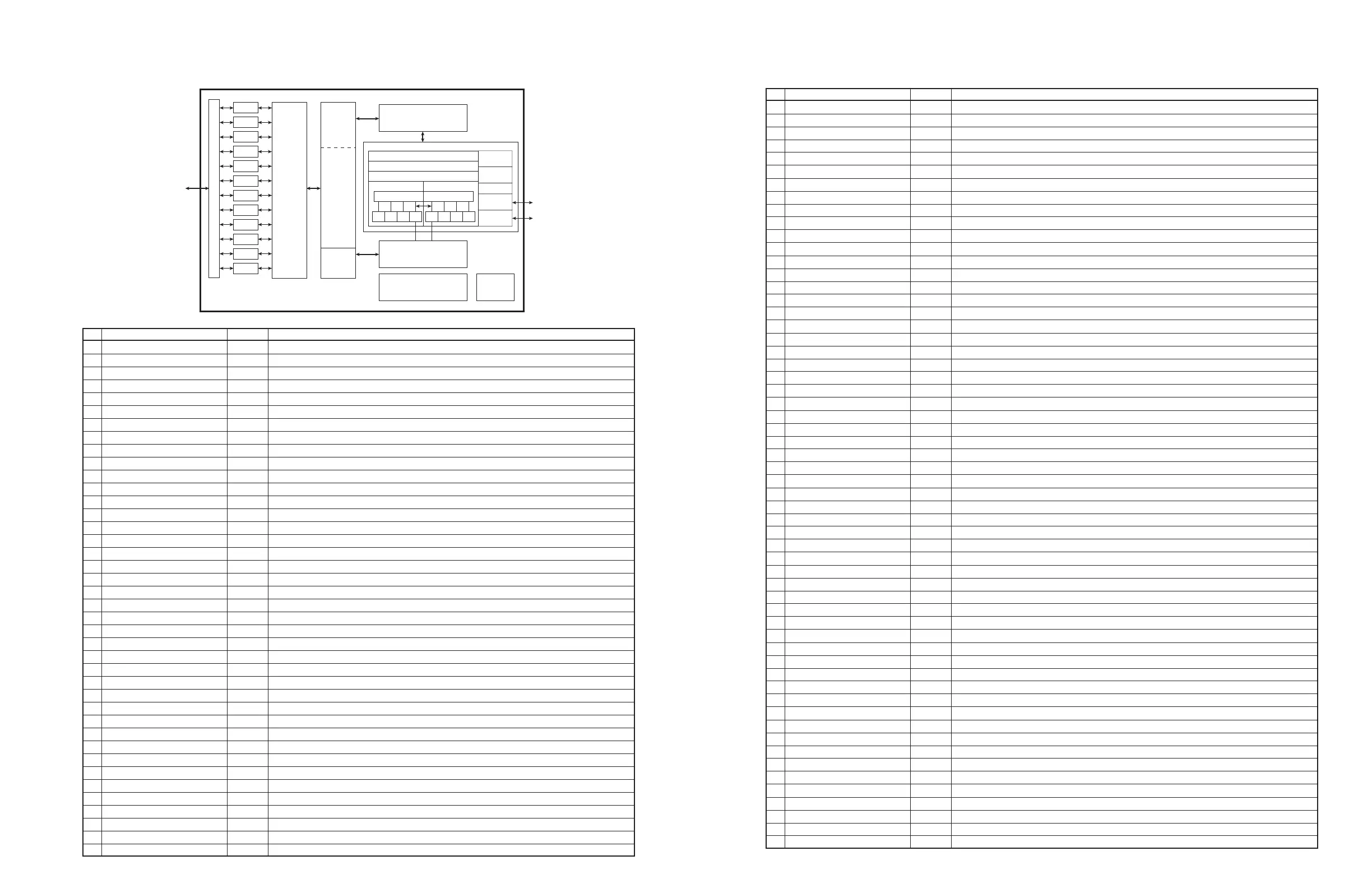
No. Name [Default] I/O Function
1 GP0[4] / (EXT_INT4) IOZ
General purpose I/O0 port 4 / Interrupt input (polarity selectable individually by using register)
2 GP0[6] / (EXT_INT6) IOZ
General purpose I/O0 port 6 / Interrupt input (polarity selectable individually by using register)
3 CVDD S 1.2V power supply
4 VSS GND Ground
5 DVDD S 3.3V power supply
6 GP0[5] / (EXT_INT5) IOZ
General purpose I/O0 port 5 / Interrupt input (polarity selectable individually by using register) (Unconnected)
7 GP0[7] / (EXT_INT7) IOZ
General purpose I/O0 port 7 / Interrupt input (polarity selectable individually by using register) (Unconnected)
8 CLKS1 I McBSP1 external clock source
9 DVDD S 3.3V power supply
10 VSS GND Ground
11 CVDD S 1.2V power supply
12 TINP1 / AHCLKX0 I / IOZ Timer 1 Input / McASP0 Transmission MCLK
13 AXR1[11] IOZ McASP1 Transmission/reception data 11
14 CVDD S 1.2V power supply
15 VSS GND Ground
16 CLKX0 / ACLKX0 IOZ McBSP0 Transmission clock / McASP0 Transmission BCLK
17 AXR1[12] IOZ McASP1 Transmission/reception data 12
18 AXR1[13] IOZ McASP1 Transmission/reception data 13
19 ACLKR0 IOZ McASP0 Reception BCLK
20 DX0 O/Z McBSP0 Transmission data
21 FSX0 IOZ McBSP0 Transmission Frame Sync
22 CVDD S 1.2V power supply
23 VSS GND Ground
24 AFSR0 IOZ McASP0 Reception LRCLK
25 DVDD S 3.3V power supply
26 VSS GND Ground
27 DR0 I McBSP0 Reception data
28 AHCLKR0 IOZ McASP0 Reception MCLK
29 CVDD S 1.2V power supply
30 VSS GND Ground
31 FSX1 IOZ McBSP1 Transmission Frame Sync (Input in SPI slave state) (Unconnected)
32 AXR1[10] IOZ McASP1 Transmission/reception data 10
33 CLKX1 / AMUTE0 IOZ
McBSP1 Transmission clock (Input in SPI slave state) / McASP0 MUTE output (Unconnected)
34 VSS GND Ground
35 CVDD S 1.2V power supply
36 AXR1[9] IOZ McASP1 Transmission/reception data 9
37 DR1 / SDA1 I / IOZ McBSP1 Reception data / I2C1 data (Unconnected)
38 AXR1[8] IOZ McASP1 Transmission/reception data 8
39 VSS GND Ground
40 CVDD S 1.2V power supply
IC512: D601A003BPYP225 (DSP P.C.B)
Decoder
No. Name I/O Function
41 SCL0 IOZ I2C0 clock
42 SDA0 IOZ I2C0 data
43 CVDD S 1.2V power supply
44 DVDD S 3.3V power supply
45 VSS GND Ground
46 CVDD S 1.2V power supply
47 DVDD S 3.3V power supply
48 VSS GND Ground
49 VSS GND Ground
50 CVDD S 1.2V power supply
51 CVDD S 1.2V power supply
52 VSS GND Ground
53 CVDD S 1.2V power supply
54 VSS GND Ground
55 DVDD S 3.3v power supply
56 ARDY I Asynchronous RAM Ready input
57 /CE3 O/Z For external memory area, Enable 3 (Unconnected)
58 DVDD S 3.3V power supply
59 VSS GND Ground
60 CVDD S 1.2V power supply
61 /CE2 O/Z For external memory area, Enable 2 (Unconnected)
62 EA2 O/Z For external memory, Address 2
63 EA3 O/Z For external memory, Address 3
64 EA4 O/Z For external memory, Address 4
65 DVDD S 3.3V power supply
66 VSS GND Ground
67 CVDD S 1.2v power supply
68 EA5 O/Z For external memory, Address 5
69 EA6 O/Z For external memory, Address 6
70 EA7 O/Z For external memory, Address 7
71 EA8 O/Z For external memory, Address 8
72 DVDD S 3.3V power supply
73 VSS GND Ground
74 EA9 O/Z For external memory, Address 9
75 /SDRAS O/Z SDRAM RAS
76 EA10 O/Z For external memory, Address 10
77 ECLKOUT O/Z Clock output for EMIF
78 ECLKIN I Clock input for EMIF (Unconnected)
79 /SDCAS O/Z SDRAM CAS
80 CVDD S 1.2V power supply
81 VSS GND Ground
82 CLKOUT2 / GP0[2] O/Z / IOZ Half clock output of device Speed / General purpose I/O0 port 2 (Unconnected)
83 /SDWE O/Z SDRAM WE
84 DVDD S 3.3V power supply
85 VSS GND Ground
86 EA11 O/Z For external memory, Address 11
87 DVDD S 3.3V power supply
88 VSS GND Ground
89 CVDD S 1.2V power supply
90 EA14 O/Z For external memory, Address 14 (Unconnected)
91 EA13 O/Z For external memory, Address 13
92 EA16 O/Z For external memory, Address 16 (Unconnected)
93 EA12 O/Z For external memory, Address 12
94 EA15 O/Z For external memory, Address 15 (Unconnected)
95 EA18 O/Z For external memory, Address 18 (Unconnected)
96 CVDD S 1.2V power supply
97 VSS GND Ground
98 DVDD S 3.3V power supply
* No service part
avilable.
※ サービス部品として供給し
ません。
 Loading...