RFSoC Data Converter Evaluation Tool User Guide 19
UG1287 (v2018.2) October 1, 2018 www.xilinx.com
Chapter 3: Hardware Design
Memory Loopback Details
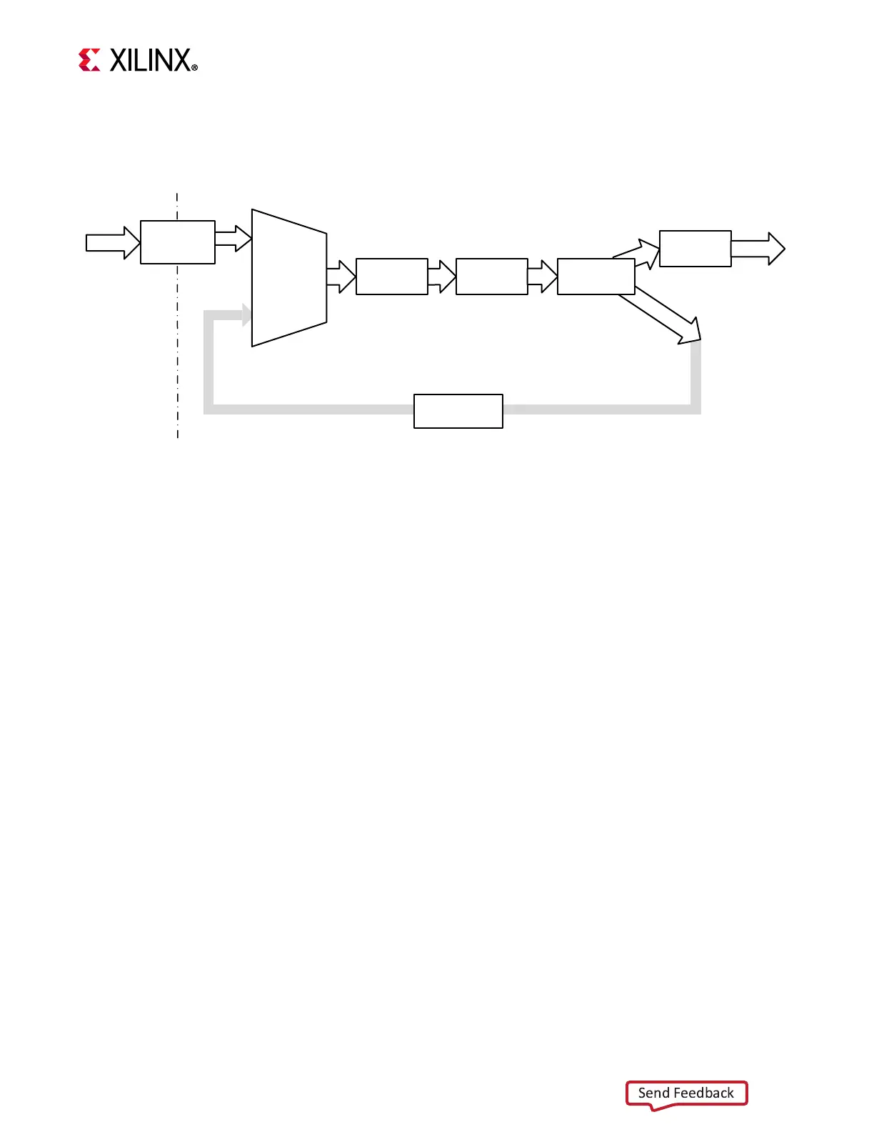
Figure 3-6 illustrates the working of memory loopback (BRAM mode) in one DAC path.
The data coming from the DMA via the AXI4-Stream decoder (Stream MUX) is fed into an
asynchronous AXI4-Stream FIFO. This takes care of the clock domain crossing between the
DMA clock and DAC clock domain. The output of the FIFO is fed into an AXI4-Stream
multiplier component. This component switches between regular BRAM (Loopback) mode
and DDR (Continuous Playback) mode. The control switch logic block takes input from
PS-GPIOs through an EMIO interface, and when it is High (controlled by software), the
output of the corresponding control logic goes High and enables the channel. The working
of the control switch is further described in the DAC Control Switch section.
Based on mode
selection, either data is continuously replayed from AXIS FIFO to the AXIS broadcaster, or data is
continuously fetched from DMA and subsequently transferred to DAC.
X-Ref Target - Figure 3-6
Figure 3-6: Implementation of Memory Loopback Component
AXIS FIFO
Control
Switch
DAC
Interface
To DAC
DAC CLK Domain
(S01)
AXIS
Broadcaster
AXIS
FIFO
AXI Stream
Mux
DMA Clock
Domain
(S00)
DMA
AXIS FIFO
X21239-092118
Loopback
 Loading...