RFSoC Data Converter Evaluation Tool User Guide 31
UG1287 (v2018.2) October 1, 2018 www.xilinx.com
Chapter 4: Clocking
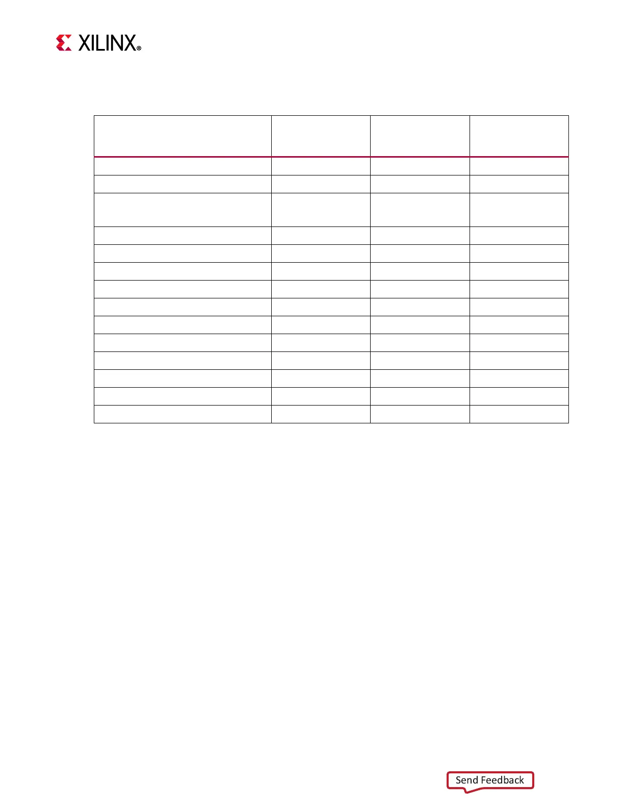
Table 4-1 lists the clocks used for the RF-ADC control path and datapath.
The RF-DAC has 300 MHz and DAC_CLK_OUT (409.625 MHz) clock domains. The
DAC_CLK_OUT is an output of RF data converter block (usp_rf_data_converter_0) and is
currently being configured to 409.625 MHz. Figure 4-7 and Figure 4-8 show the RF-DAC
clock domains.
Table 4-1: Clock Domains in RF-ADC Control and Datapath
Logic Block
ADC Stream
Clock Domain
(512 MHz)
Clock Domain
(300 MHz)
ADC Clock Domain
(256 MHz)
ADC (usp_rf_data_converter) X
Channel select multiplexer X
FIFO (axis_data_fifo_0) (ADC 0-ADC7)
Asynchronous FIFO
X (WRITE Clock) X (READ Clock)
DMA (axi_dma) X
AXI interconnect (AXI smart connect) X
PL DDR controller interface X
ADC_0 I & Q Merge X
ADC_1 I & Q Merge X
ADC_2 I & Q Merge X
ADC_3 I & Q Merge X
ADC_4 I & Q Merge X
ADC_5 I & Q Merge X
ADC_6 I & Q Merge X
ADC_7 I & Q Merge X
 Loading...