T-1
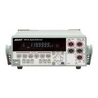
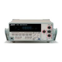
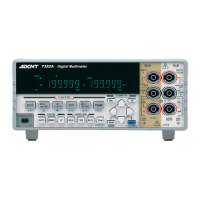
7451A/7461A/7461P Digital Multimeter Operation Manual
LIST OF TABLES
No. Title Page
3-1 Standard Accessories ........................................................................................................ 3-2
3-2 ESD Countermeasures ...................................................................................................... 3-4
3-3 Accessories ....................................................................................................................... 3-5
3-4 Relation Table between AC Power Supply Voltage and Indication of Set Power Supply Voltage 3-8
4-1 Maximum Allowable Applied Voltage (DCV) ................................................................ 4-6
4-2 Range and Input impedance (DCV) .................................................................................. 4-6
4-3 Maximum Allowable Applied Voltage (DCV-Bch) ......................................................... 4-7
4-4 Range and Input impedance .............................................................................................. 4-7
4-5 Selecting the AC Filter ..................................................................................................... 4-8
4-6 Maximum Allowable Applied Voltage (ACV and ACV(AC+DC)) ................................ 4-8
4-7 Measurement range ........................................................................................................... 4-9
4-8 Maximum Allowable Applied Voltage (2W, 4W, LP-2W, LP-4W) .................... 4-10
4-9 Selecting the AC Filter ..................................................................................................... 4-12
4-10 Measurement Range .........................................................................................................4-13
4-11 Continuity Measurement ................................................................................................... 4-14
4-12 Diode Measurement .......................................................................................................... 4-15
4-13 Maximum Allowable Applied Voltage (FREQ) ............................................................... 4-16
4-14 Temperature Measurement ............................................................................................... 4-17
4-15 Display Resolution ............................................................................................................ 4-17
4-16 Sampling Rate, Measurement Speed, and Auto-Zero ....................................................... 4-19
4-17 Sampling Rate and Display Digits .................................................................................... 4-20
5-1 Menu Operation Key and Function .................................................................................. 5-3
5-2 Measurement Function and Range Structure .................................................................... 5-11
5-3 Performing Auto-Zero ...................................................................................................... 5-13
5-4 Setting Range and Resolution of the Integration Time (IT) ............................................. 5-16
5-5 Setting Range of Sampling Interval (SI) ........................................................................... 5-17
5-6 Integration Time and Minimum Measurement Time ....................................................... 5-17
5-7 Trigger Delay Time, Setting Resolution, and Accuracy ................................................... 5-23
5-8 Delta Trigger Detection Pattern ........................................................................................ 5-27
5-9 Relationship according to Disabling the Function ............................................................ 5-49
6-1 Interface Functions ........................................................................................................... 6-3
6-2 Standard Bus Cable ........................................................................................................... 6-4
6-3 Optical Semiconductor Relay Contact and TTL Logical Output (a) ................................ 6-12
6-4 Optical Semiconductor Relay Contact and TTL Logical Output (b) ................................ 6-12
6-5 ADC Commands ...............................................................................................................6-13
6-6 SCPI Commands ............................................................................................................... 6-14
6-7 Status Byte Register (STB) ............................................................................................... 6-49
6-8 Standard Event Status Register (SESR) ............................................................................ 6-51
6-9 Measurement Event Register (MER) ................................................................................ 6-52
6-10 Questionable Event Register (QER) ................................................................................. 6-53
6-11 Operation Event Register (OER) ...................................................................................... 6-54
7-1 Options .............................................................................................................................. 7-22