User’s Manual
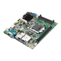
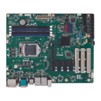
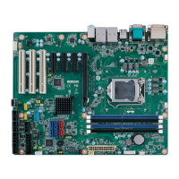
AIMB-240 Series User’s Manual
63
DRAM timing parameter from On-DIMM’s SPD device. (default is by SPD)
3.5.3.2 CAS Latency Time (changeable when DRAM Timing Selectable setting is Manual)
This item controls the time delay (in clock cycles - CLKs) that passes before the SDRAM
starts to carry out a read command after receiving it. This also determines the number of
CLKs for the completion of the first part of a burst transfer. In other words, the lower the
latency, the faster the transaction.
The available options are: 2, 2.5.
3.5.3.3 Active to Precharge Delay (changeable when DRAM Timing Selectable setting is Manual)
This item is the minimum delay time between Active and Precharge
The available options are: 5, 6, 7.
3.5.3.4 DRAM RAS# to CAS# Delay (changeable when DRAM Timing Selectable setting is Manual)
This option allows you to insert a delay between the RAS (Row Address Strobe) and CAS
(Column Address Strobe) signals. This delay occurs when the SDRAM is written to, read
from or refreshed. Naturally, reducing the delay improves the performance of the SDRAM
while increasing it reduces performance.
The available options are: 2, 3.
3.5.3.5 DRAM RAS# Precharge (changeable when DRAM Timing Selectable setting is Manual)
This option sets the number of cycles required for the RAS to accumulate its charge before
the SDRAM refreshes. Reducing the precharge time to 2 improves SDRAM performance
but if the precharge time of 2 is insufficient for the installed SDRAM, the SDRAM may not
be refreshed properly and it may fail to retain data
So, for better SDRAM performance, set the SDRAM RAS Precharge Time to 2 but
increase it to 3 if you face system stability issues after reducing the precharge time.
The available options are: 2, 3.
3.5.3.6 DRAM Data Integrity Mode
(changeable when DRAM Timing Selectable setting is Manual)
Select ECC if your memory module supports it. The memory controller will detect and
correct single-bit soft memory errors. The memory controller will also be able to detect
double-bit errors though it will not be able to correct them. This provides increased data
integrity and system stability.
The available options are: Non-ECC, ECC.
3.5.3.7 MGM Core Frequency
This field sets the frequency of the DRAM memory installed.
The available options are: Auto Max 266MHz, 400/266/133/200 MHz, 400/200/100/200
MHz, 400/200/100/133 MHz, 400/266/133/267 MHz, 533/266/133/200 MHz,
533/266/133/266 MHz, 400/333/166/250 MHz, Auto Max 400/333 MHz,
Auto Max 533/333 MHz.
3.5.3.8 System BIOS Cacheable
This feature is only valid when the system BIOS is shadowed. It enables or disables the
caching of the system BIOS ROM at F0000h-FFFFFh via the L2 cache. This greatly
speeds up accesses to the system BIOS. However, this does not translate into better