The +12V generates the FPGA core power supply through the DCDC power supply chip IS6608, and the output
current is up to 60A, which can meet the current demand of the core voltage. The +12V power supply supplies
power to the FPGA auxiliary power supply and the high-speed transceiver through three DCDC chips: SGM61163
generates VCCAUX, and IS66066 generates MGTAVCC and MGTAVTT power supplies. At the same time, the +12V
power supply generates +1.2V through the DCDC chips ETA1471 and SGM61163. The VCC1V8_FPGA and D3V3
power supplies power to the BANK and peripherals of DDR4 and FPGA. In addition, D3V3 generates the auxiliary
power supply of the high-speed transceiver and the ADC power supply +1.8V of the FPGA through two LDO chips
ETA5060; the VTT and DDR2V5 voltages of DDR4 are generated by TPS51200 and ETA5050.
Because the power supply of FPGA has the requirement of power-on sequence, in the circuit design, we have
designed according to the power supply requirements of the chip to ensure the normal work of the chip.
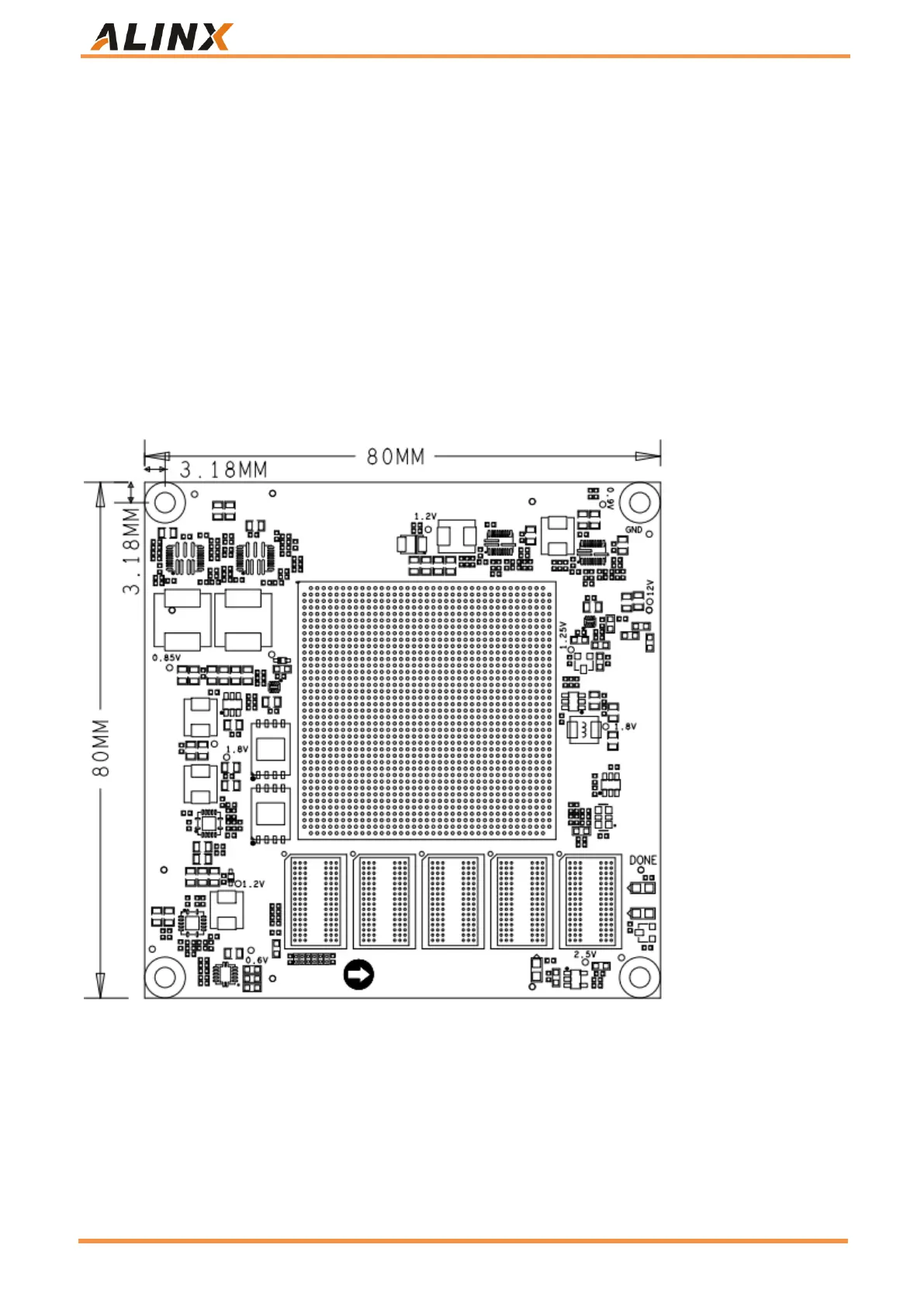
Part 2.8: Structure Diagram
Figure 15: Top View
Part 2.9: Connector pin definition
The module is extended with four high-speed expansion ports, which are connected to the base board by four
240Pin inter-board connectors (J1 ~ J4), and the power supply of the module is input by the J3 connector.
 Loading...


