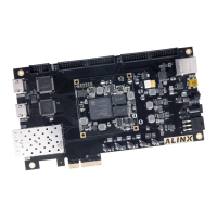
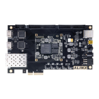
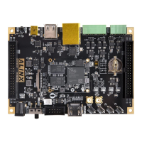
Part 3: Base board
Part 3.1: Introduction
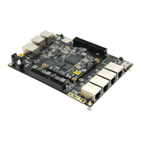
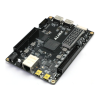
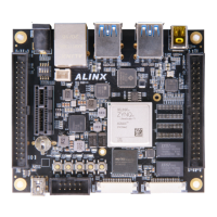
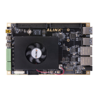
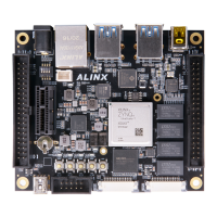
Through the previous function introduction, we can understand the functions of the base board.
⚫ PCIe3.0 x16 interface
⚫ 1 * Gigabit network interface
⚫ 2 * FMC HPC interface
⚫ 2 * MIPI input interface
⚫ USB Uart interface
⚫ Micro SD deck
⚫ 2 * STATA interface
⚫ 40-pin expansion port
⚫ JTAG debug port
⚫ Led light
⚫ Key
Part 3.2: PCIe Slot
There is a PCIe x16 interface on the AXKU15 base board, which supports PCIe Gen3.0 protocol, and 8 pairs of
transceivers are connected to the golden finger of PCIEx16 for data communication.
The receiving and transmitting signals of the PCIe interface are directly connected to the FPGA BANK228 ~ 231
transceivers. The 16-channel TX signals and RX signals are connected to the FPGA transceivers in the form of
differential signals. The communication rate of a single channel can be as high as 8G bit bandwidth.
The design diagram of the PCIe interface of the development board is shown in Figure 16 below, in which the TX
transmission signal is connected in AC coupling mode.


 To Next Page