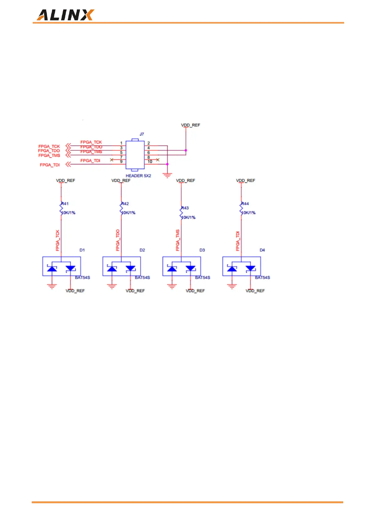
Part 3.13: JTAG Debugging port
A 10-PIN JTAG interface is reserved on the AXKU15 base board for downloading FPGA programs or solidifying
programs to FLASH. To avoid the damage to the FPGA chip caused by live plugging, we add a protection diode on
the JTAG signal to ensure that the voltage of the signal is within the acceptable range of the FPGA, to avoid the
damage to the chip.
Figure 30: JTAG Interface Part in Schematic Diagram
Part 3.14: Power source
The power input voltage of the development board is DC12V, which can supply power to the board through the
PCIE slot or external +12V power supply. Please use the power supply provided by the development board when
supplying power from the external power supply. Do not use the power supply of other specifications to avoid
damaging the development board. The 3-channel DC/DC power supply chip SGM61163 outputs +5V, FMC2 _
VADJ and 3.3V voltage respectively; ETA1471 outputs FMC1_VADJ regulated voltage. The +3.3V output at the same
time is the voltage required by each FPGA BANK of the multiple LDO output JTAG.
The power supply design diagram on the board is shown in Figure 31 below:
 Loading...