EasyManua.ls Logo

Alinx AXKU15 - Part 3.4: FMC HPC Interface

Alinx AXKU15
51 pages
Print Icon
To Next Page IconTo Next Page
To Previous Page IconTo Previous Page
Loading...
AXKU15 User Manual
www.en.alinx.com
The FPGA pin assignments for the Ethernet PHY are as follows:
Signal name
FPGA pin number
Remark
ETH_MDC
AW10
MDIO manages the clock
ETH_MDIO
AW11
MDIO manages data
ETH_RESET
AM18
PHY chip reset
ETH_RXCK
AK17
RGMII receive clock
ETH_RXCTL
AL17
Receive data valid signal
ETH_RXD0
AL16
Receive data Bit0
ETH_RXD1
AK16
Receive data Bit1
ETH_RXD2
AU12
Receive data Bit2
ETH_RXD3
AP13
Receive data Bit3
ETH_TXCK
AR11
RGMII transmit clock
ETH_TXCTL
AN13
Send enable signal
ETH_TXD0
AJ14
Send data bit0
ETH_TXD1
AK14
Send data bit1
ETH_TXD2
AU13
Send data bit2
ETH_TXD3
AV13
Transmit data bit 3
Table 17: Ethernet PHY pin assignment
Part 3.4: FMC HPC Interface
The development board is equipped with two FMC HPC expansion ports, namely FMC1 (J12) and FMC2 (J13), which
can be externally connected with XILINX or various FMC modules of Alinx (HDMI input and output module,
binocular camera module, high-speed AD module, etc.).
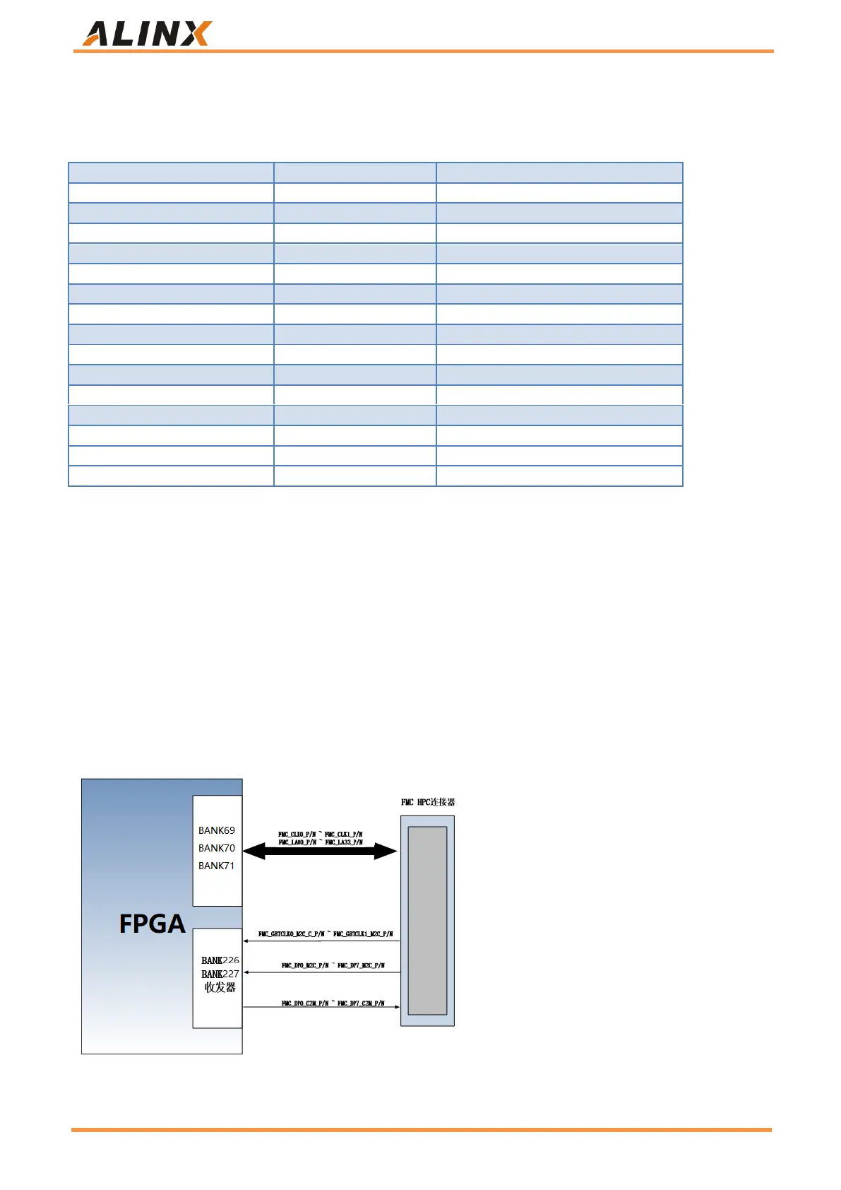
The FMC1 expansion port includes 34 pairs of LA signal differential pairs, 2 pairs of clock signals and 24 pairs of HA
signals, which are respectively connected to the FPGA chips BANK69, BANK70 and BANK71. The standard level is
1.8V by default. 8 channels of high-speed GTY transceiving signals are connected to the IO of FPGA chips
BANK226 and BANK227.
The schematic diagram of the FPGA and FMC HPC connector is shown in Figure 19:
Figure 19: Connection Schematic Diagram of FMC HPC Interface

Related product manuals