network transmission rate and communicates with FPGA through RGMII interface. JL21221D chip supports
MDI/MDX self-adaptation, various speed self-adaptation and Master/Slave self-adaptation and supports register
management of PHY by MDIO bus.
When the JL21221D is powered on, it will detect the level status of some specific IOs to determine its own working
mode. Table 16 describes the default setting information after the GPHY chip is powered on.
Default configuration values of PHY chip:
Table 16: PHY chip configuration
When the network is connected to Gigabit Ethernet, the data transmission between FPGA and PHY chip JL2121 is
communicated through RGMII bus. The transmission clock is 125Mhz, and the data is sampled at the rising edge
and falling edge of the clock.
When the network is connected to 100M Ethernet, the data transmission of FPGA and PHY chip JL2121 is
communicated through RMII bus, and the transmission clock is 25 Mhz. Data is sampled on the rising and falling
edges of the clock.
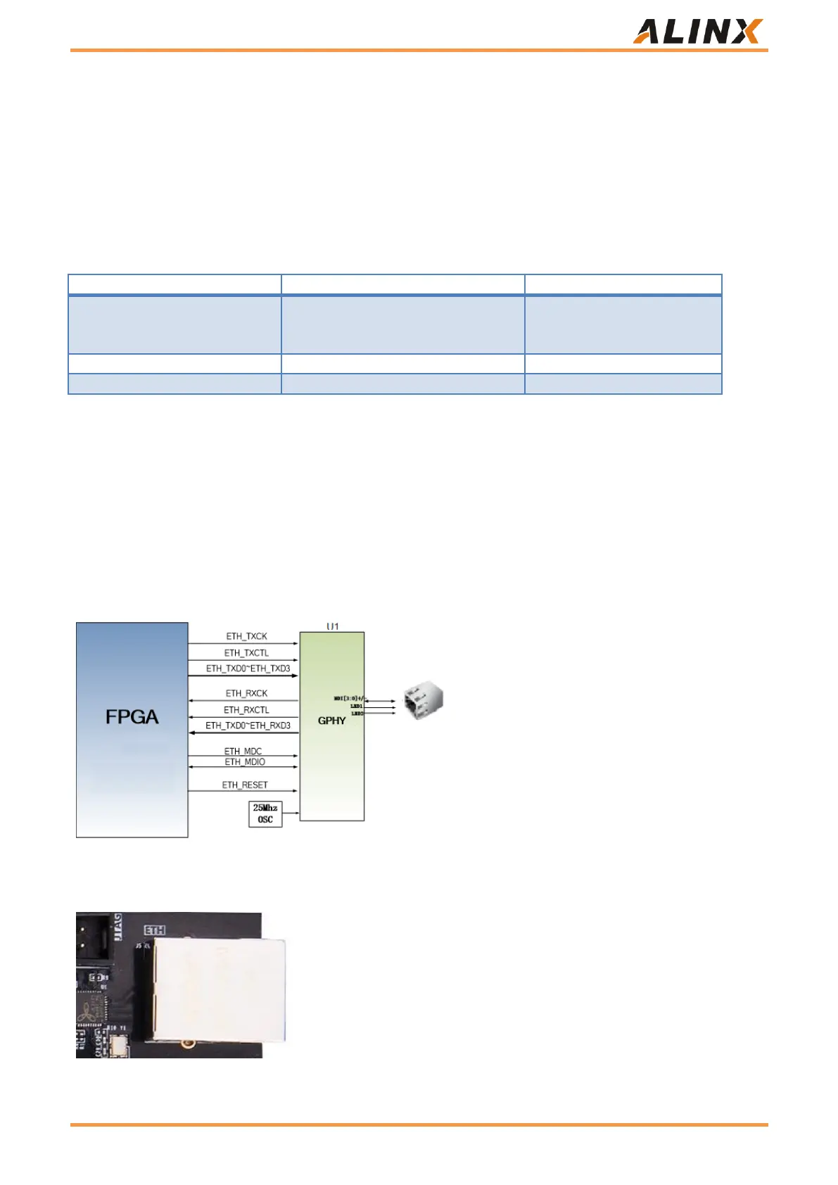
Figure 17 shows the connection between FPGA and Ethernet PHY chip:
Figure 17: Connection Schematic Diagram of Gigabit Network Interface
Figure 18 is the physical diagram of the Ethernet PHY chip.
Figure 18: Physical Diagram of Ethernet PHY Chip
 Loading...