Part 2.3: DDR4
The ACKU15 SOM module is equipped with five Micron 1GB DDR4 chips, model MT40A512M16LY-062 E, which are
connected to the HP side of the FPGA to form an 80-bit data bus with a capacity of 5GB. The maximum running
data rate of DDR4 SDRAM on the FPGA side is 2,666Mbps, and five DDR4 memory systems are directly connected
to the memory interfaces of BANK 66, 67 and 68. The specific configuration of DDR4 SDRAM is shown in Table 2
below.
Table 2: DDR4 SDRAM Configuration
The hardware design of DDR4 needs to strictly consider the signal integrity. We have fully considered the
matching resistor/termination resistor, trace impedance control, and trace length control in the circuit design and
PCB design to ensure the high-speed and stable operation of DDR4.
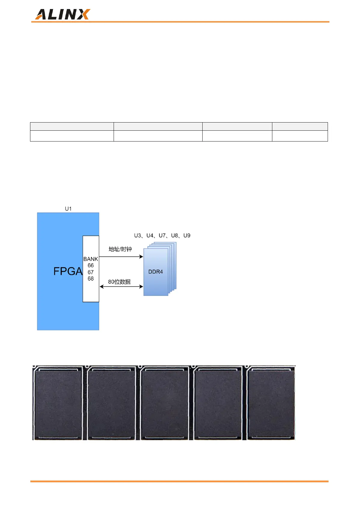
The hardware connection mode of DDR4 on the FPGA side is shown in Figure 6:
Figure 6: DDR4 DRAM Schematic
Figure 7 shows the physical picture of two DDR4 DRAMs of the development board.
Figure 7: Physical drawing of 4 DDR4 DRAM
 Loading...