www.en.alinx.com
www.en.alinx.com
Table 23: SD card slot pin assignment
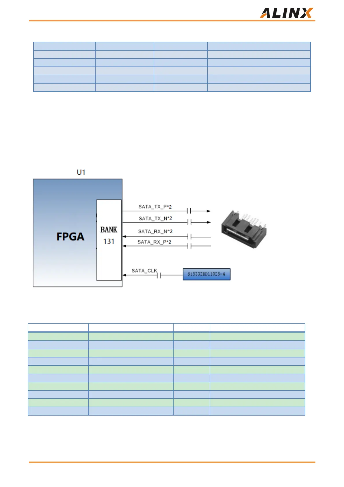
Part 3.8: SATA Interface
The board is equipped with two SATA interfaces, and the differential signal of SATA is connected to GTY BANK131.
The SATA reference clock of 150Mhz is provided by the programmable clock chip Si5332BD11025-4. The schematic
diagram of SATA interface design is shown in Figure 25 below:
Figure 25: SATA Interface Design Diagram
The SATA interface FPGA pin assignments are as follows:
SATA1 data receive negative
SATA 1 data receiving positive
SATA2 data reception is negative
SATA2 data receiving positive
SATA 1 Data Transmit Negative
SATA 1 Data Sending Positive
SATA2 data transmission is negative
SATA2 Data Sending Positive
SATA Reference Clock Negative
SATA reference clock positive
Table 24: SATA interface pin assignment
 Loading...