LM75a sensor pin assignment:
Table 27: LM75a sensor pin assignment
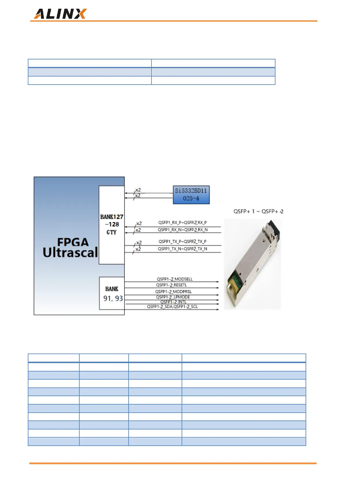
Part 3.12: Fiber Optic Interface
There are two QSFP28 optical fiber interfaces on the base board, and the user can purchase a QSFP optical
module to be inserted into the four optical fiber interfaces for optical fiber data communication. The two optical
interfaces are respectively connected with the four RX/TX of the GTY transceiver of BANK127-128 of the FPGA. The
reference clock of BANK127-128 can be provided by Si5332BD11025-4 chip or independent crystal oscillator.
The schematic diagram of FPGA and optical fiber design is shown in Figure 29 below:
Figure 29: Schematic diagram of fiber design
The 2-way optical interface pins are assigned as follows:
Optical module 1 data reception minus 1
Optical module 1 data receiving positive 1
Optical module 1 data receiving negative 2
Optical module 1 data receiving positive 2
Optical module 1 data receiving negative 3
Optical module 1 data receiving positive 3
Optical module 1 data receiving negative 4
Optical module 1 data receiving positive 4
Optical module 1 data sending minus 1
Optical module 1 data sending positive 1
 Loading...