Part 2: ACKU15 SOM Module
Part 2.1: Introduction
ACKU15 (SOM model, the same below) SOM module, FPGA chip is based on the Xilinx FPGA Kintex Ultrascale+
main chip XCKU15PFFVE1517 design. The module connects five DDR4 memory chips to the HP port of the FPGA to
form an 80-bit data bandwidth, and the capacity of each DDR4 chip is up to 1GB. Memory bandwidth on the HP
side is up to 210Gb/s. In addition, two QSPI FLASHs of 512MBit size are integrated on the module, which are used
to start storage configuration and system files.
This module expands 256 HPIOs and 88 HDIOs by using a board-to-board connector. The level of the outgoing IO
can be modified by replacing the LDO chip on the base board to meet the user's requirement of not using a level
interface. In addition, the module also expands 24 pairs of GTY and 32 pairs of GTH high-speed transceiver
interfaces. This module will be a good choice for users who need a lot of IO and high-speed transceivers.
Moreover, in the IO connection part, the wiring between the FPGA chip and the interface is processed with equal
length and difference, and the size of the module is only 80 * 80 (mm), which is very suitable for secondary
development.
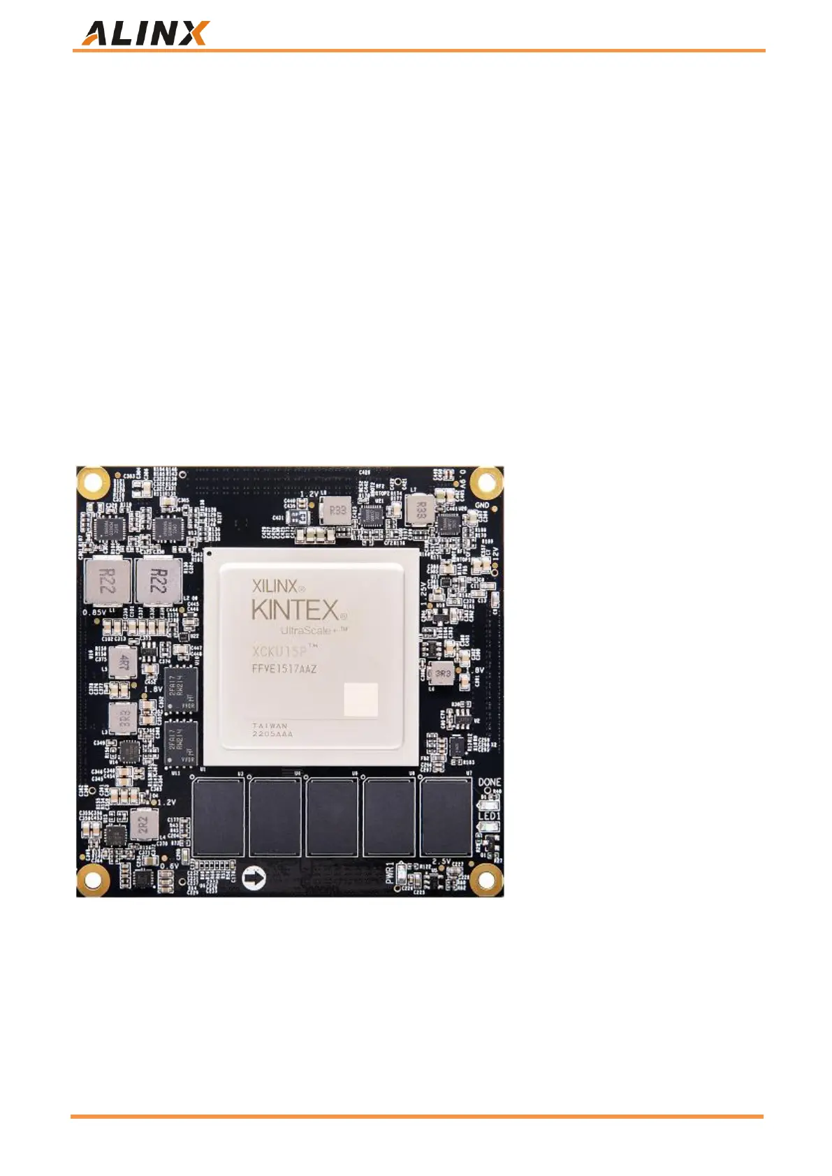
Figure 3: Front View of ACKU15 Module
Part 2.2: FPGA Chip
As mentioned above, the model of the FPGA we used is XCKU15PFFVE1517, which belongs to the Kintex
Ultrascale+ series of Xilinx, with a speed grade of 2 and an industrial temperature grade. This model is in the
FFVE1517 package with 1517 pins. The chip naming rule of Xilinx Kintex Ultrascale+ FPGA is as follows: